Method of manufacturing semiconductor device

a manufacturing method and semiconductor technology, applied in the direction of semiconductor devices, basic electric elements, electrical equipment, etc., can solve the problems of tungsten plug short circuit and increase the connection resistance of tungsten plugs

Inactive Publication Date: 2008-05-01
ELPIDA MEMORY INC
View PDF6 Cites 181 Cited by
  • Summary
  • Abstract
  • Description
  • Claims
  • Application Information

AI Technical Summary

Benefits of technology

[0008]An object of the present invention is to provide a method of manufacturing a se...

Problems solved by technology

If a timing at which the process is ended is too late, a connection resistance of the tungsten plug will increase because of excessive polis...

Method used


Image

  • Method of manufacturing semiconductor device
  • Method of manufacturing semiconductor device
  • Method of manufacturing semiconductor device

Examples


first embodiment

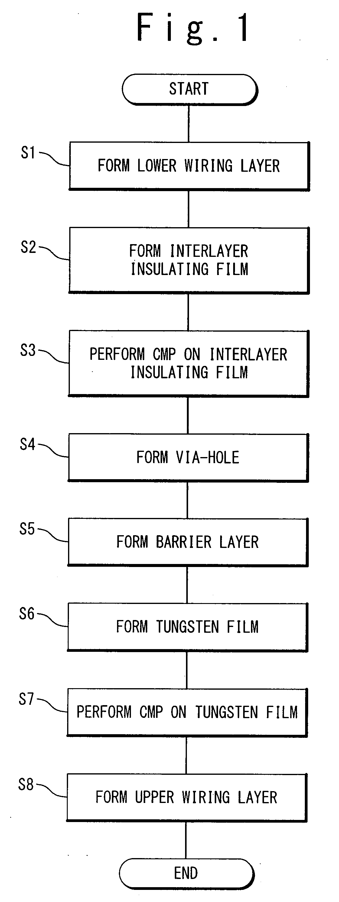
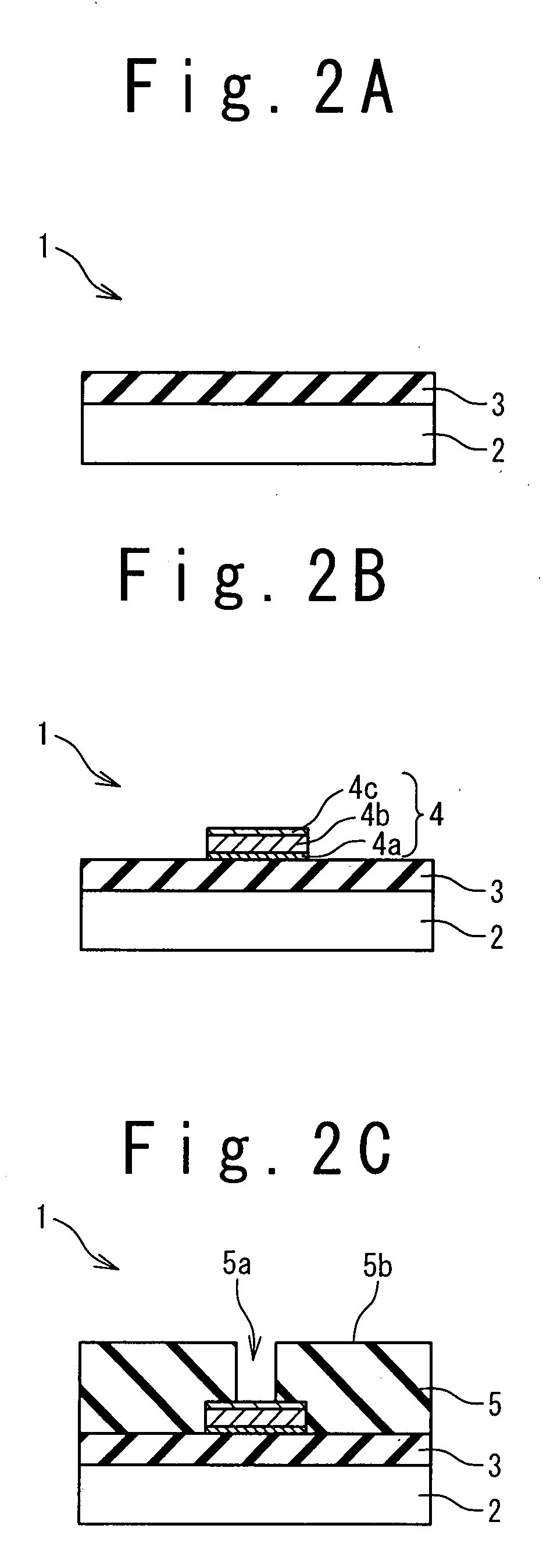
[0032]First, an outline of the method of manufacturing the semiconductor device according to the present invention will be described with reference to FIG. 1 and FIGS. 2A to 2F.

[0033]FIG. 1 is a flowchart showing the method of manufacturing the semiconductor device according to the first embodiment of the present invention. FIG. 1 shows a process of forming multiple wiring layers on a semiconductor wafer 1 on which transistors have been formed. After the multiple wiring layers are formed, a passivation film is formed on the semiconductor wafer 1, which is then diced into a plurality of semiconductor chips. Each semiconductor chip is mounted on a lead frame, each terminal of the lead frame is connected with one electrode pad of the semiconductor chip, and the semiconductor chip is molded with resin. Then, a semiconductor device (semiconductor integrated circuit) is completed by passing through a test process. As the semiconductor devices, a volatile memory, a nonvolatile memory, and ...

second embodiment

[0065]Next, a modification example of the method of manufacturing the semiconductor device according to the present invention will be described with reference to FIGS. 13 and 14.

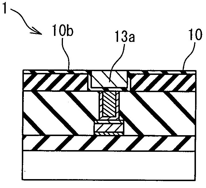
[0066]FIG. 13 is a flowchart showing a modification example of the method of manufacturing the semiconductor device according to the second embodiment of the present invention. Steps S9 to S14 shown in FIG. 13 are performed instead of the step S8 shown in FIG. 1. The steps S9 to S14 are a process of forming an upper wiring layer 13a instead of the upper wiring layer 8. The upper wiring layer 13a is a copper interconnection formed by a damascene method.

[0067]FIGS. 14A to 14D are sectional views of the semiconductor wafer to show a process of forming the upper wiring layer 13a in the method of manufacturing the semiconductor device according to the second embodiment of the present invention.

[0068]At the step S9, an insulating layer 9 is formed on the semiconductor wafer 1 shown in FIG. 2E. The insulating film ...


PUM


Abstract

In a method of manufacturing a semiconductor device, an insulating film with a concave portion is formed on a semiconductor wafer. A barrier layer is formed on the insulating film to cover a surface of the insulating film such that the barrier layer has a uniform crystal orientation over a whole wafer surface of the semiconductor wafer. A metal film is formed on the barrier layer such that a portion of the metal film fills the concave portion, and a CMP (Chemical Mechanical Polishing) method is performed on the metal film to leave the filling portion of the metal film.

Description

BACKGROUND OF THE INVENTION[0001]The present invention relates to a method of manufacturing a semiconductor device, and more particularly, to a method of manufacturing multi-level interconnection.[0002]A low-resistance metal plug is used to connect a lower wiring layer and an upper wiring layer in a semiconductor device. The metal plug such as a tungsten plug is formed as follows. First, a barrier layer including a titanium film (Ti film) and a titanium nitride film (TiN film) are formed on an interlayer insulating film in which via-holes are formed. Subsequently, a tungsten film (W film) is formed on the barrier layer by a CVD (Chemical Vapor Deposition) method. Subsequently, an extra portion of the tungsten and barrier films on the flat surface of the interlayer insulating film is removed by a CMP (Chemical Mechanical Polishing) method so that the barrier layer and the tungsten film filling the via-hole are left.[0003]In the above method of forming the tungsten plug, it is importa...

Claims


Application Information

Patent Timeline
IPC IPC(8): H01L21/44
CPCH01L21/2855H01L21/7684H01L21/76843H01L2924/0002H01L2924/00
Inventor SAITO, MASAYOSHI
Owner ELPIDA MEMORY INC
Why Eureka
Try Eureka