Method of fabricating organic thin film transistor using self assembled monolayer-forming compound containing dichlorophosphoryl group

a thin film transistor and dichlorophosphoryl group technology, applied in the field of organic thin film transistors, can solve the problems of increasing on-current drop, reducing the contact resistance with the upper organic semiconductor, and unsatisfactory processibility, and achieve the effect of improving electrical properties

Inactive Publication Date: 2008-05-08
SAMSUNG ELECTRONICS CO LTD
View PDF3 Cites 35 Cited by
  • Summary
  • Abstract
  • Description
  • Claims
  • Application Information

AI Technical Summary

Benefits of technology

[0011]Accordingly, example embodiments have been made keeping in mind the above problems occurring in the related art, and example embodiments provide a method of fabricating an OTFT, in which the surface of the metal oxide source / drain electrodes or the surface of the metal oxide source / drain electrodes and gate electrode is treated with an SAM-forming compound containing a dichlorophosphoryl group able to form a covalent bond with metal oxide, so that the work function of the metal oxide is higher than that of the organic semiconductor material, thus resulting in improved electrical properties, including increased charge mobility. Example embodiments provide an OTFT, fabricated using the method. Example embodiments provide a display device, fabricated using the OTFT.

Problems solved by technology

Because gold (Au) has a work function similar to an organic semiconductor, improved organic semiconductor properties may be manifested, but may have undesirable processibility when compared with other metals.
However, metal oxides, for example, ITO, have a work function different from that of the organic semiconductor, and therefore a Schottky barrier is formed between the metal oxide electrode and the organic semiconductor layer, undesirably resulting in increased on-current drop.
Because most of the insulating layer or electrodes of the OTFT are formed of metal oxide, the above technique may decrease the contact resistance with the upper organic semiconductor.
However, as illustrated in FIG. 1, because the above material is formed into a film on metal oxide through physical adsorption, it may undesirably be dissociated from the metal oxide at increased temperatures or in an increased vacuum.
However, this material may self-oligomerize due to moisture present in the air, and thus, may be difficult to apply to mass production lines.
As another covalently bondable SAM material, a compound in which a monochlorophosphoryl group is introduced to the side chain of a polymer, may suffer because it does not play a sufficient role in forming the SAM attributable to the presence of only one reactive group.

Method used


Image

  • Method of fabricating organic thin film transistor using self assembled monolayer-forming compound containing dichlorophosphoryl group
  • Method of fabricating organic thin film transistor using self assembled monolayer-forming compound containing dichlorophosphoryl group
  • Method of fabricating organic thin film transistor using self assembled monolayer-forming compound containing dichlorophosphoryl group

Examples


example 1

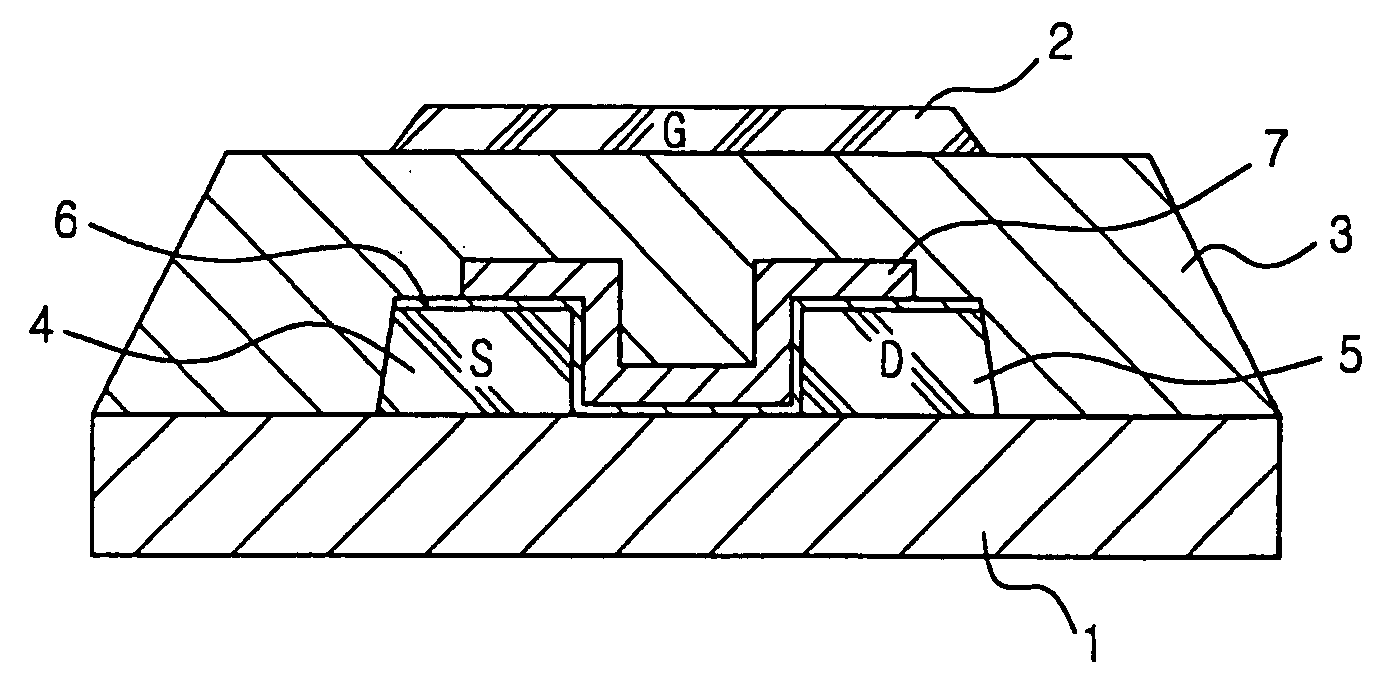
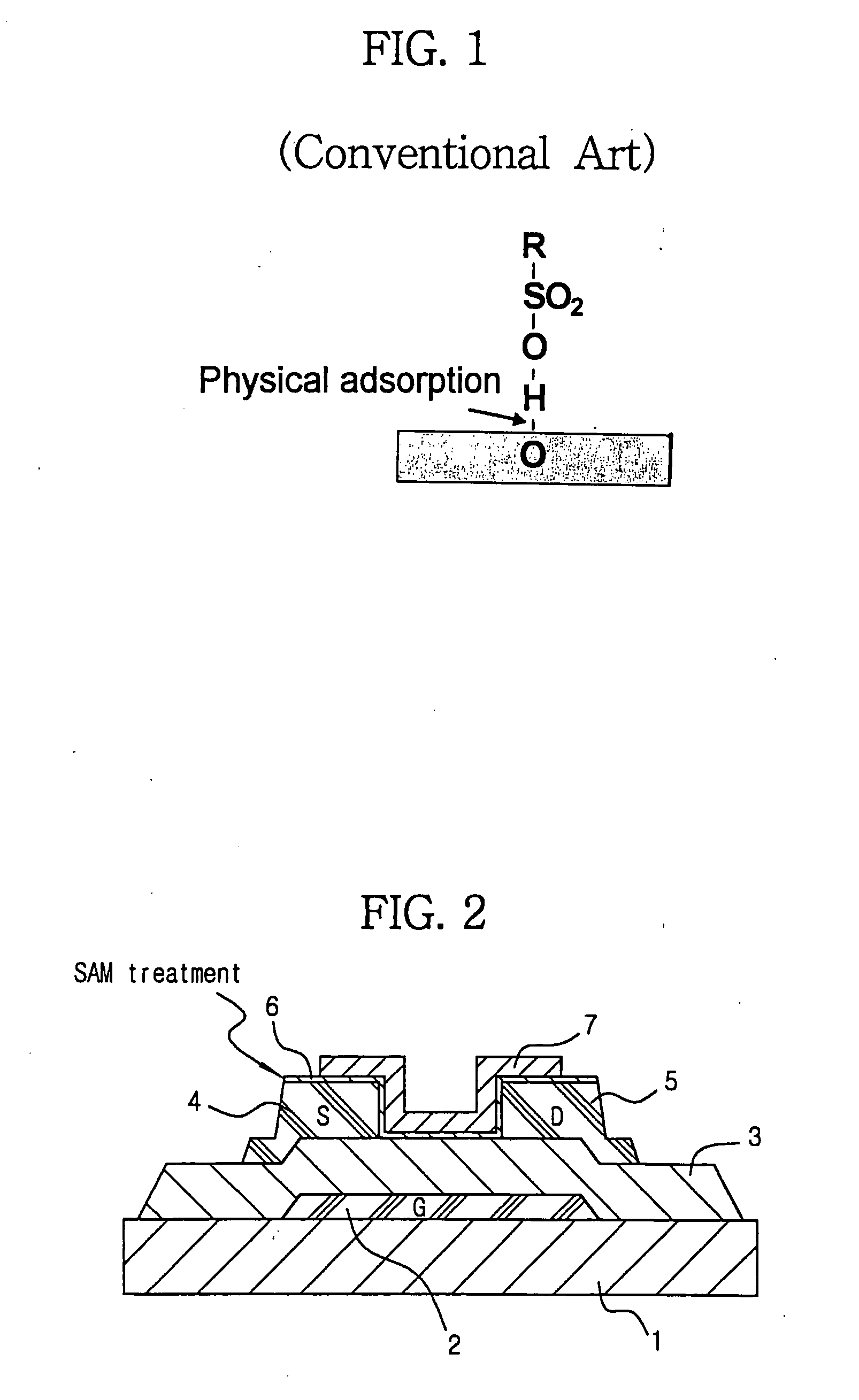
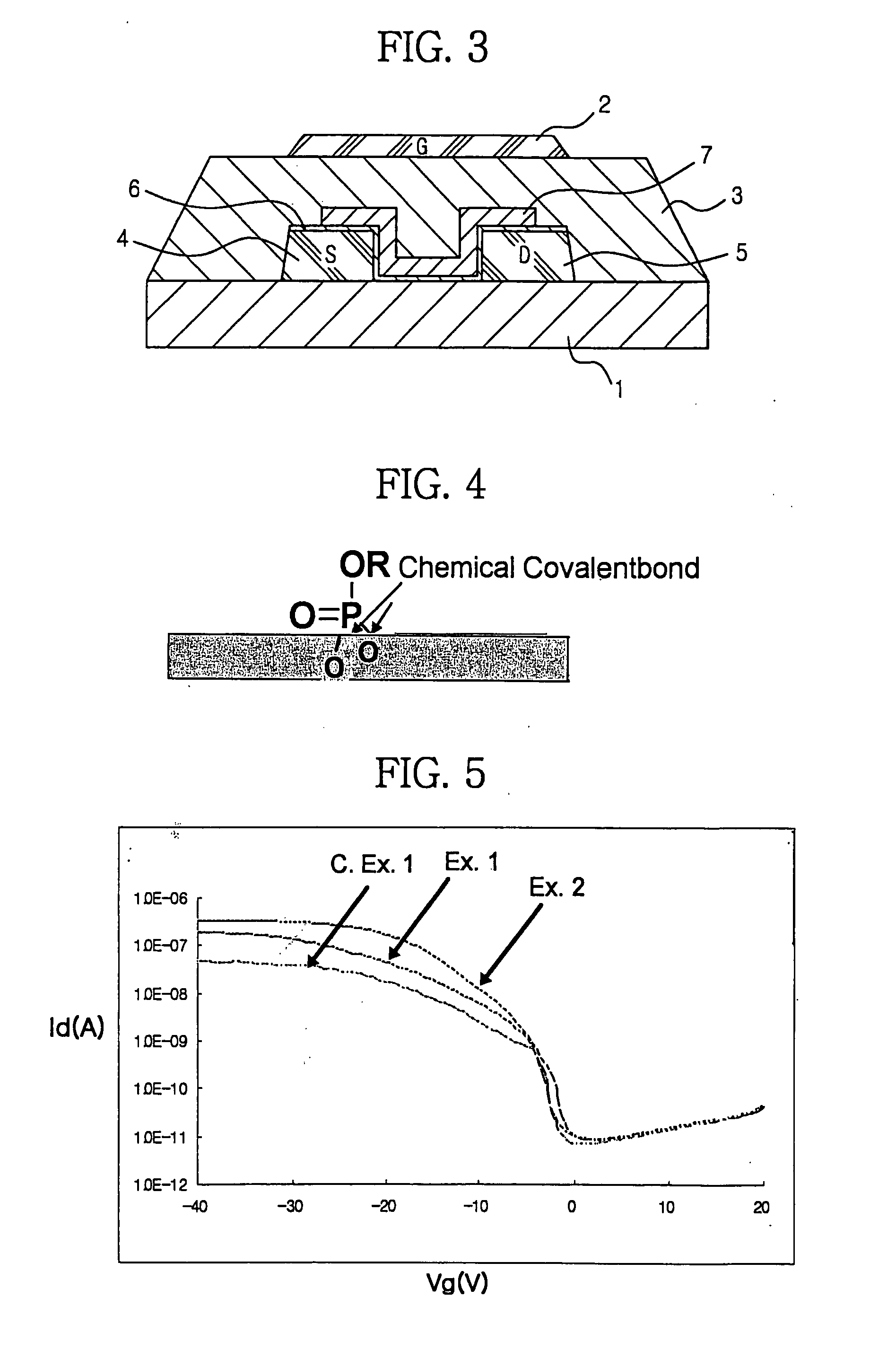
[0061]On a washed glass substrate, a gate electrode was formed to a thickness of about 1500 Å through sputtering using Al / Nd. Subsequently, a PVP-based insulator was applied to a thickness of about 5000 Å on the gate electrode through spin coating at about 1000 rpm to thus form a gate insulating layer, which was then subjected to soft baking at about 100° C. for about 5 min, resulting in a desired gate insulating layer. ITO was deposited to a thickness of about 1000 Å thereon through thermal evaporation under a vacuum condition (about 2×10⁻⁷ torr, substrate temperature of about 50° C., and deposition rate of about 0.85 Å / sec), followed by performing photolithography to thus form an ITO electrode pattern. Thereafter, the ITO electrode was immersed in an SAM-forming solution, obtained by dissolving an SAM-forming compound represented by Formula 16 below in about 0.2 wt % ethyl alcohol, at room temperature for about 10 sec to thus realize surface treatment, and was then annealed for ab...

example 2

[0062]An OTFT was fabricated in the same manner as in Example 1, with the exception that a compound containing a dichlorophosphoryl group having fluorine, represented by Formula 17 below, was used as the SAM-forming compound:


PUM

PropertyMeasurementUnit
timeaaaaaaaaaa
charge mobilityaaaaaaaaaa
semiconductor propertiesaaaaaaaaaa

Abstract

Disclosed is a method of fabricating an organic thin film transistor including a substrate, a gate electrode, a gate insulating layer, metal oxide source/drain electrodes, and an organic semiconductor layer, in which the surface of the metal oxide source/drain electrodes or of the metal oxide source/drain electrodes and gate insulating layer is treated with a self assembled monolayer-forming compound containing a dichlorophosphoryl group. According to the method of example embodiments, the work function of the metal oxide of the source/drain electrodes may be increased to be higher than that with no SAM-forming electrode, thus making it possible to fabricate an improved organic thin film transistor having increased charge mobility.

Description

PRIORITY STATEMENT[0001]This non-provisional application claims priority under U.S.C. § 119 to Korean Patent Application No. 2006-107677, filed on Nov. 02, 2006, in the Korean Intellectual Property Office (KIPO), the entire contents of which are herein incorporated by reference.BACKGROUND[0002]1. Field[0003]Example embodiments relate to a method of fabricating an organic thin film transistor (OTFT) using a self assembled monolayer (SAM)-forming compound containing a dichlorophosphoryl group. Other example embodiments relate to a method of fabricating an OTFT including a substrate, a gate electrode, a gate insulating layer, metal oxide source / drain electrodes, and an organic semiconductor layer, in which the surface of the metal oxide source / drain electrodes or of the metal oxide source / drain electrodes and gate insulating layer is treated with an SAM-forming compound containing a dichlorophosphoryl group, so that the work function of the metal oxide of the source / drain electrodes is...

Claims


Application Information

Patent Timeline
Patent Type & Authority Applications(United States)
IPC IPC(8): H01L51/40C07D333/02C07F9/08H01L29/08
CPCC07F9/14C07F9/1406C07F9/5722H01L51/105C07F9/655345H01L51/0541C07F9/65515C07F9/572H10K10/464H10K10/84
Inventor JEONG, EUN JEONGHAHN, JUNG SEOKPARK, JEONG ILLEE, SANG YOON
Owner SAMSUNG ELECTRONICS CO LTD
Why Eureka
Try Eureka