Cascode low noise amplifier with a source coupled active inductor

active inductor technology, applied in the field of low noise amplifiers, can solve the problems of complex process of manufacturing spiral inductor on-chip, large chip area, and unrealistic applications, and achieve the effects of reducing the nf of a rf low noise amplifier, reducing the chip size and increasing the high frequency gain of a low noise amplifier

Inactive Publication Date: 2008-05-15
NATIONAL TSING HUA UNIVERSITY
View PDF5 Cites 15 Cited by
  • Summary
  • Abstract
  • Description
  • Claims
  • Application Information

AI Technical Summary

Benefits of technology

[0009] Another object of the present invention is to reduce the chip size of a low noise amplifier.
[0010] Yet another object of the present invention is to decrease the NF of a RF low noise amplifier.
[0011] Still another object of the present invention is to increase the high frequency gain of a low noise amplifier.
[0012] According to the present invention, a low noise amplifier comprises a pair of cascode transistors, among which is an input transistor having a source coupled with an active inductor. The low noise amplifier can be equivalent to three current sources coupled in series, and the active inductor introduces a transconductance such that the NF is reduced and the gain is increased. Since the active inductor replaces the on-chip spiral inductor, the size of the low noise amplifier is reduced. The active inductor can further provide input impedance matching for the low noise amplifier.

Problems solved by technology

However, the on-chip spiral inductor requires greater chip area, and its quality factor Q is restricted, so being unrealistic in applications.
Further, the process of manufacturing the on-chip spiral inductor is complicated, requires higher cost, and is difficult to control the inductance of the on-chip spiral inductor.
There also have been proposed to use micro electro-mechanical system (MEMS) process and other materials to improve the on-chip spiral inductor, but the effect on reducing the chip area is not significant, and the cost still cannot be reduced because the number of photomasks is increased and the elements become fragile.
However, there are still some disadvantages when using active inductor, and the worst case is that it brings greater noise, so it can be only used in low-frequency circuits, but not appropriate to high-frequency circuits.
Furthermore, the cost of BiCMOS process is very high, it is doubtful that using BiCMOS active inductor could save cost, and the performance could be good enough.
However, replacing the load inductor which is coupled to the output of the low noise amplifier by an active inductor causes greater noise, so it also can be only used in low frequency circuits.

Method used


Image

  • Cascode low noise amplifier with a source coupled active inductor
  • Cascode low noise amplifier with a source coupled active inductor
  • Cascode low noise amplifier with a source coupled active inductor

Examples


Embodiment Construction

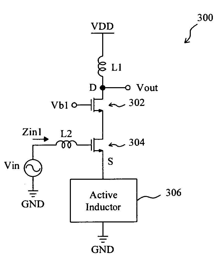
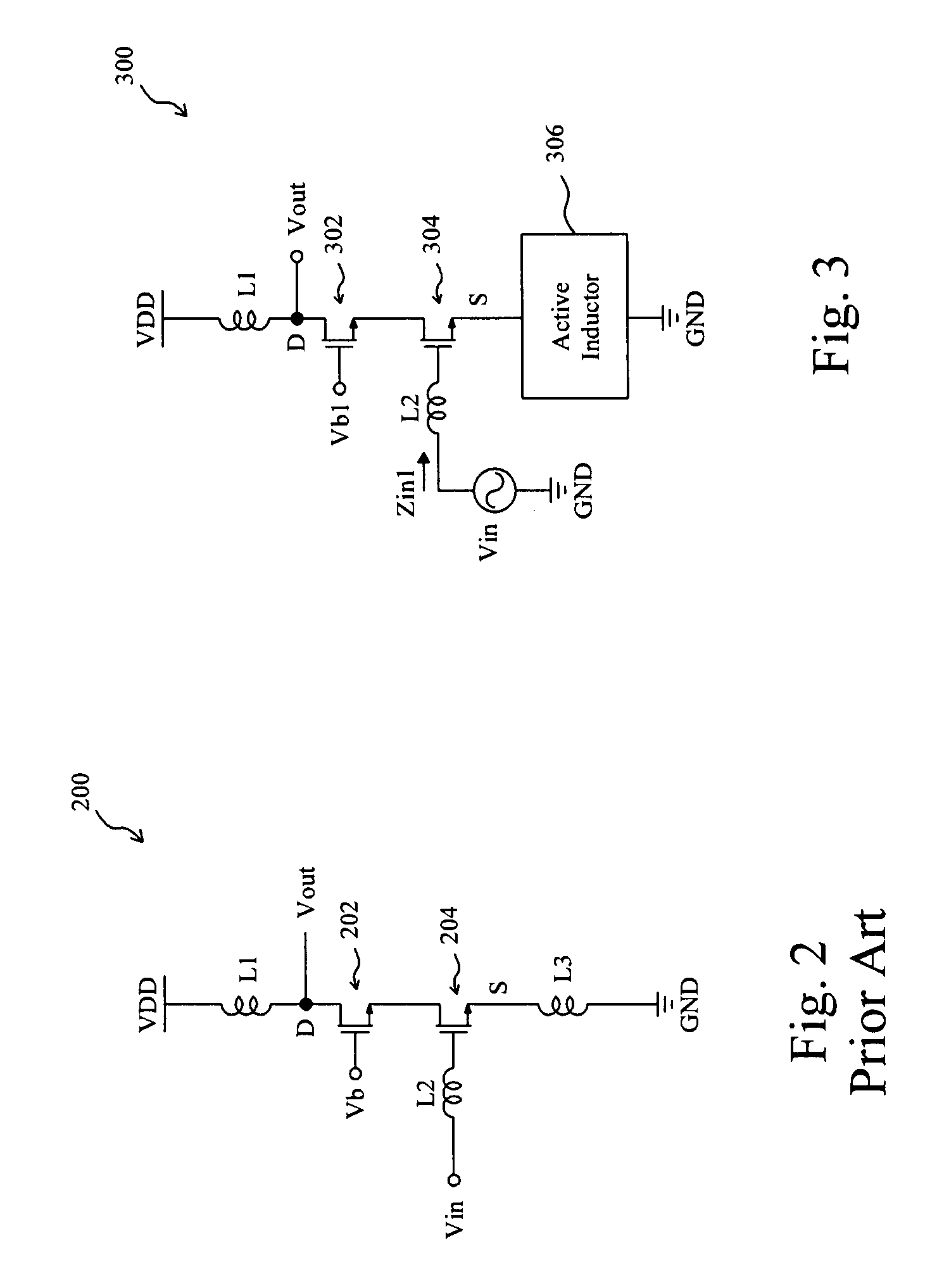
[0028]FIG. 3 provides a cascode low noise amplifier 300 according to the present invention, which comprises a pair of cascode transistors 302 and 304, and a load inductor L1 coupled to the drain D of the output transistor 302. The drain D of the output transistor 302 is also the output of the low noise amplifier 300 to provide the output signal Vout, and the gate of the output transistor 302 is coupled with a bias voltage Vb1. The input transistor 304 has a gate coupled with an input signal Vin through an input inductor L2, and a source S coupled with an active inductor 306. The input impedance seen from the input Vin is Zin1. Preferably, all the elements 302, 304 and 306 are integrated into a same chip. Either one of the inductors L1 and L2 may be an external wire-wound inductor, an on-chip spiral inductor, or an active inductor. If the load inductor L1 is an on-chip spiral inductor or an active inductor, it can be also integrated with the elements 302, 304 and 306 into the same ch...


PUM


Abstract

A cascode low noise amplifier includes an input transistor and an output transistor cascode together, the input transistor has a source coupled to an active inductor, and the output transistor has a drain to provide an output signal. By using the active inductor, the low noise amplifier has smaller size, lower noise figure, and higher gain. The active inductor also provides input impedance matching for the low noise amplifier.

Description

FIELD OF THE INVENTION [0001] The present invention is related generally to a low noise amplifier (LNA) and, more particularly, to a cascode low noise amplifier employing active inductor. BACKGROUND OF THE INVENTION [0002] In recent years, applications of wireless communications become popular quickly. For example, cell phones, wireless networks, and satellite phones have been widely used by people in their lives. Therefore, the needs of communications significantly increase, and the competition in international markets is intense. To provide a technology standard for the manufacturers to design their products, the Institute of Electrical and Electronics Engineers (IEEE) issues the IEEE 802.11 specification in 1997, which defines the physical layer (PHY layer) and media access control layer (MAC layer), and also defines the radio frequency (RF) band of 2.4 GHz, in which the data transfer rate is up to 2 Mbps. Then, the 802.11a specification focuses on industry, science and medicine ...

Claims


Application Information

Patent Timeline
Patent Type & Authority Applications(United States)
IPC IPC(8): H03F3/68
CPCH03F1/223H03F1/565H03F3/19H03F3/195H03F3/345H03F2200/489H03F2200/181H03F2200/222H03F2200/294H03F2200/451H03F2200/108
Inventor GONG, JENGHUANG, I-LUN
Owner NATIONAL TSING HUA UNIVERSITY
Why Eureka
Try Eureka