Coating Compositions for Use in Forming Patterns and Methods of Forming Patterns

a technology of coating composition and forming pattern, which is applied in the field of coating composition for use in forming pattern and methods of forming pattern, can solve the problems of increasing the difficulty of developing semiconductor devices using next-generation materials, increasing the difficulty of forming fine contact holes, and increasing the difficulty of dry etching and/or line edge roughness, so as to improve the durability against dry etching

Inactive Publication Date: 2008-05-15
SAMSUNG ELECTRONICS CO LTD
View PDF6 Cites 73 Cited by
  • Summary
  • Abstract
  • Description
  • Claims
  • Application Information

AI Technical Summary

Benefits of technology

[0015] Example embodiments of the present invention provide coating compositions for forming etch mask patterns, usable in forming fine patterns. Coating compositions according to example embodiments of the present invention may overcome a wavelength limitation in a lithography process by forming an overcoating layer having an improved durability against dry etching.
[0016] Example embodiments of the present invention also provide methods of forming fine patterns having a smaller feature size, which may improve the durability against dry etching, line edge roughness (LER) characteristics, reduce the deformation of the sidewall profiles of apertures, and / or create a fine pattern having a smaller feature size.
[0017] The coating composition according to example embodiments of the present invention may be used in a lithography process for forming a fine pattern used in semiconductor devices such that improved durability against dry etching may be obtained and / or LER may be reduced. In addition, a fine pattern having a smaller feature size may be effectively achieved by reducing the deformation of the side wall profiles of apertures.

Problems solved by technology

However, due to material and / or process limitations, developing semiconductor devices using next generation materials has become increasingly difficult.
For example, in the ArF laser lithography process, components, layers, etc., may be susceptible to dry etching and / or line edge roughness (LEG).
In addition, forming a fine contact hole may be increasingly difficult using related art photolithography processes.
For example, a contact hole having a size smaller than 100 nm may be more difficult to achieve because a contact hole pattern has lower resist resolution than a line and space pattern.
As a result, a bowing profile and / or swelling may occur.
Accordingly, because the flow rate of the photoresist pattern may be more difficult to control when the above-described example method is used, it may be more difficult to decrease the CD while maintaining the vertical pattern profile.
Although the differences in the CD may be reduced for a contact hole pattern having a uniform size and / or duty, it may be more difficult to reduce the deformation of the pattern shape at pattern edges and applications of the TFP may be limited.
In RELACS, however, because the solubility of the water-soluble polymer and the crosslinker to the deionized water is limited, an organic solvent such as IPA is utilized.
When developed using only the deionized water, defects may be generated on a substrate.
As a result, the process may become more complicated and / or expensive.
Although the RELACS may be used in an ArF lithography process, defects remain after the process and / or susceptibility to dry etching remains.
Reducing CD according to the related art techniques may be more difficult when a light source having a wavelength of 153 nm or 196 nm as an exposure light source is used, and / or when the size of a hole or a trench to be obtained decreases.

Method used


Image

  • Coating Compositions for Use in Forming Patterns and Methods of Forming Patterns
  • Coating Compositions for Use in Forming Patterns and Methods of Forming Patterns
  • Coating Compositions for Use in Forming Patterns and Methods of Forming Patterns

Examples


example 1

Synthesis of a Polymer for a Coating Composition (I)

[0051]

[0052] In Example 1, 6 g (50 mmol) of Novolak resin (Mw=9,200) and 7 g (50 mmol) of potassium carbonate were dissolved in 50 ml of acetone in a round bottom flask, and 2.7 g (25 mmol) of 2-chloroethyl vinyl ether was slowly dropped in the solution. The mixture was reacted for about 12 hours.

[0053] After the reaction, the obtained precipitations were removed, the reacted materials were slowly precipitated in water, and then the obtained precipitations were filtrated. The filtrated precipitations were dissolved again in a proper amount of THF solution and were slowly precipitated again in an n-hexane solution. The obtained precipitations were dried at about 50° C. for about 24 hours in a vacuum oven. The yield was 85%.

[0054] The result had a weight average molecular weight (Mw) of 11,500 daltons and a polydispersity (Mw / Mn) of 2.6.

example 2

Synthesis of a Polymer for a Coating Composition (II)

[0055]

[0056] In Example 2, 6 g (50 mmol) of poly 4-hydroxy styrene (Mw=10,000) and 7 g (50 mmol) of potassium carbonate were dissolved in 50 ml of acetone in a round bottom flask, and 2.7 g (25 mmol) of 2-chloroethyl vinyl ether was slowly dropped in the solution. The mixture was reacted for about 12 hours.

[0057] After the reaction, the obtained precipitations were removed, the reacted materials were slowly precipitated in water, and then the obtained precipitations were filtrated. The filtrated precipitations were dissolved again in a proper amount of THF solution and were slowly precipitated again in an n-hexane solution. The obtained precipitations were dried at about 50° C. for about 24 hours in a vacuum oven. The yield was 87%.

[0058] The result had a weight average molecular weight (Mw) of 12,500 daltons and a polydispersity (Mw / Mn) of 1.6.

example 3

Evaluation of Lithography (I)

[0059] In Example 3, 1 g of the polymer of Example 1 was dissolved in 40 g of n-butanol and filtrated though a membrane filter of 0.2 μm, to obtain a coating composition for overcoating.

[0060] Anti-reflective coating (ARC) material (such as an ArF Anti-reflective coating) for an exposure wavelength of 193 nm was spin-coated on an 8-inch bare silicon wafer, and baked to form an ARC layer having a thickness of about 240 Å.

[0061] A photoresist used for an exposure wavelength of 193 nm was spin-coated on the ARC layer, and pre-baked at 110° C. for 60 seconds, to form a photoresist layer.

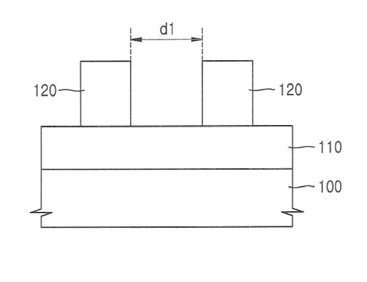
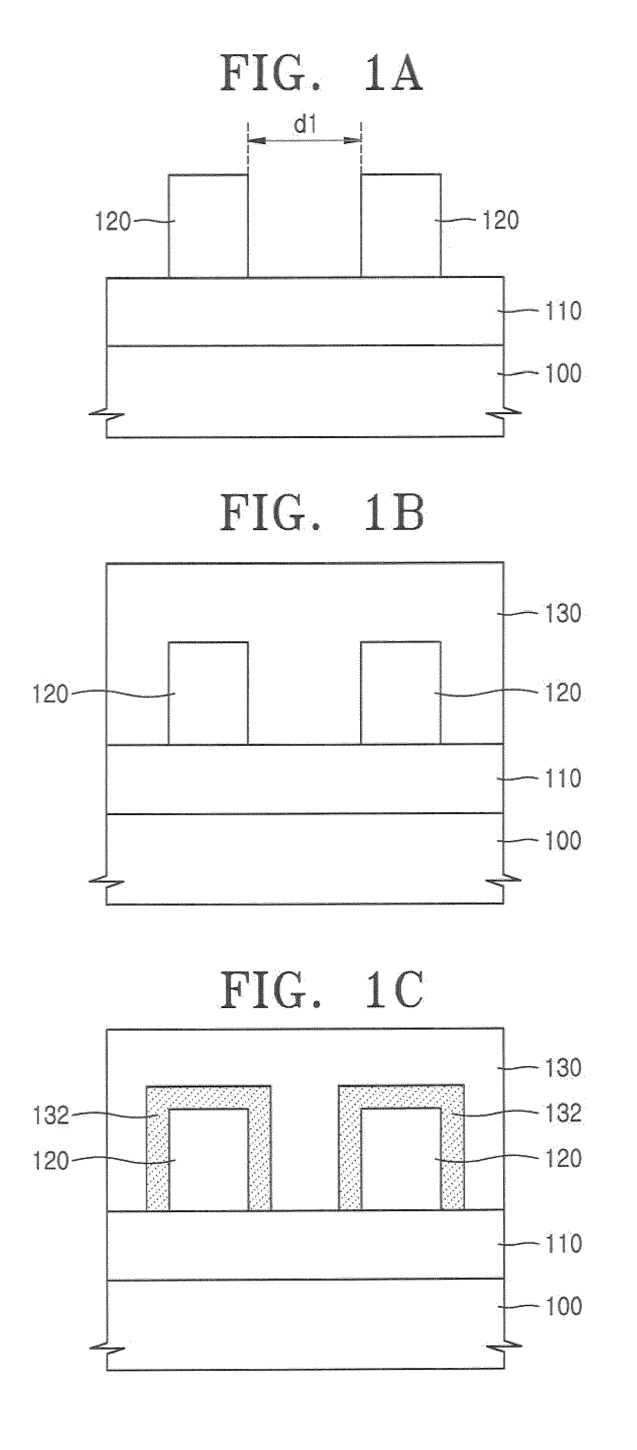
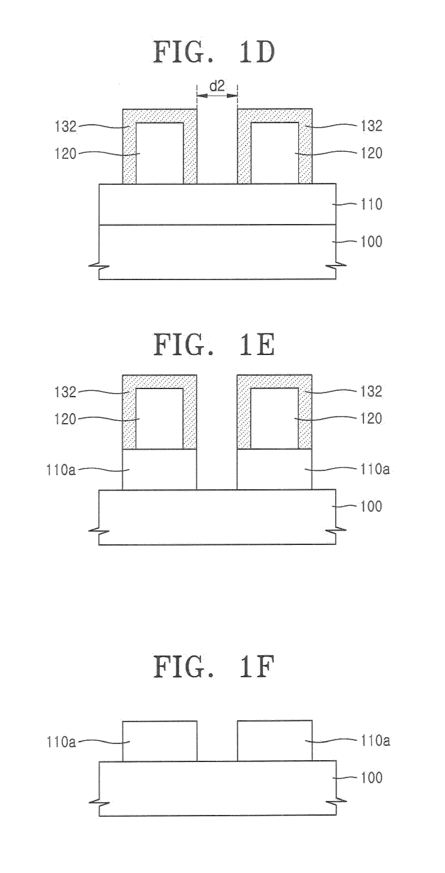
[0062] The surface of the wafer was exposed to an ArF excimer laser using an ArF scanner with NA=0.75 annular and σ=0.85 / 0.55, subjected to post-exposure bake (PEB) at 110° C. for 60 seconds, and developed with a 2.38% tetramethylammonium hydroxide solution for 60 seconds. When a dose was 30 mJ / cm2, a resist pattern having a contact hole pattern with a hole diameter of ab...


PUM

PropertyMeasurementUnit
wavelengthaaaaaaaaaa

Abstract

A coating composition for forming etch mask patterns may include a polymer and an organic solvent. The polymer may have an aromatic ring substituted by a vinyl ether functional group. The polymer may be, for example, a Novolak resin partially substituted by a vinyl ether functional group or poly(hydroxystyrene) partially substituted by a vinyl ether functional group.

Description

PRIORITY STATEMENT [0001] This application claims priority under 35 U.S.C. § 119 to Korean Patent Application No. 10-2005-0080616, filed on Aug. 31, 2005, in the Korean Intellectual Property Office (KIPO), the entire contents of which are incorporated herein by reference. BACKGROUND OF THE INVENTION [0002] 1. Field of the Invention [0003] Example embodiments of the present invention relate to coating compositions for forming etch mask patterns used in manufacturing semiconductor devices, and methods of forming fine patterns in semiconductor devices using the coating composition. [0004] 2. Description of the Related Art [0005] In related art methods of forming patterns, a photoresist pattern may be formed on an etch target layer (e.g., a silicon layer, an insulation layer or a conductive layer). The etch target layer may be etched using the photoresist pattern as an etch mask. [0006] As semiconductor devices become increasingly integrated, smaller critical dimensions (CD) may be need...

Claims


Application Information

Patent Timeline
Patent Type & Authority Applications(United States)
IPC IPC(8): G03C5/00
CPCG03F7/40H01L21/31144H01L21/0273G03F7/027G03F7/00
Inventor CHOI, SANG-JUNHATA, MITSUHIRORYOO, MAN-HYOUNGHAH, JUNG-HWAN
Owner SAMSUNG ELECTRONICS CO LTD
Why Eureka
Try Eureka