Method for passivation of plasma etch defects in DRAM devices

a technology of dram devices and passivation methods, applied in the direction of semiconductor devices, basic electric elements, electrical equipment, etc., can solve the problems of poor device yield and performance, low retention time, and challenge the ability to fabricate efficient dram devices

Inactive Publication Date: 2008-05-29
TECH SEMICON SINGAPORE PTE
View PDF10 Cites 7 Cited by
  • Summary
  • Abstract
  • Description
  • Claims
  • Application Information

AI Technical Summary

Problems solved by technology

Unwanted defects in portions of the semiconductor substrate will result in charge leakage, low retention time, and thus poor device yield and performance.
Unfortunately several semiconductor device fabrication procedures can create defects in semiconductor substrates thus challenging the ability to fabricate efficient DRAM devices.
Plasma dry etching processes such as reactive ion etching (RIE), specifically high density plasma procedures performed to define many critical features in scaled down (smaller geometries) semiconductor devices, can result in damage in the form of defect generation at semiconductor substrate.
These defects lead to unsaturated chemical bonds at the semiconductor surface promoting charge leakage from storage elements of a DRAM device.
The data retention time loss or charge leakage mechanisms suffered by DRAM devices can be in the form of junction leakage and defect assisted gate induced drain leakage (GIDL).
Numerous attempts at improving data retention time have focused on semiconductor substrate defect reduction, however most of these works involve major and costly process or design modification.
Prior art such as Schmitt et al U.S. Pat. No. 4,332,627, as well as Colombo et al US Pat. No. US2004 / 0127000 A1, teach methods of eliminating process induced defects via use high temperature anneals after arsenic processing, however these prior art result in arsenic being driven into the semiconductor substrate away from the top surface where plasma etch induced defects are formed.

Method used


Image

  • Method for passivation of plasma etch defects in DRAM devices
  • Method for passivation of plasma etch defects in DRAM devices
  • Method for passivation of plasma etch defects in DRAM devices

Examples


Embodiment Construction

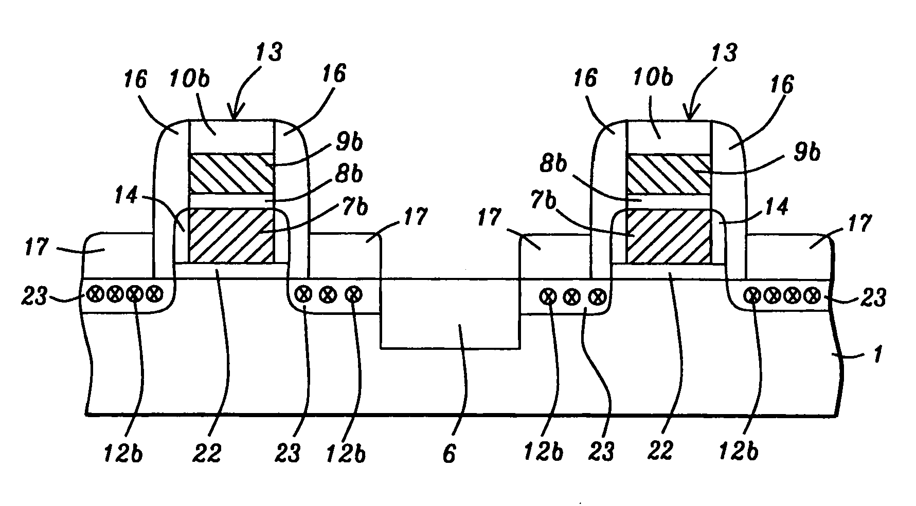
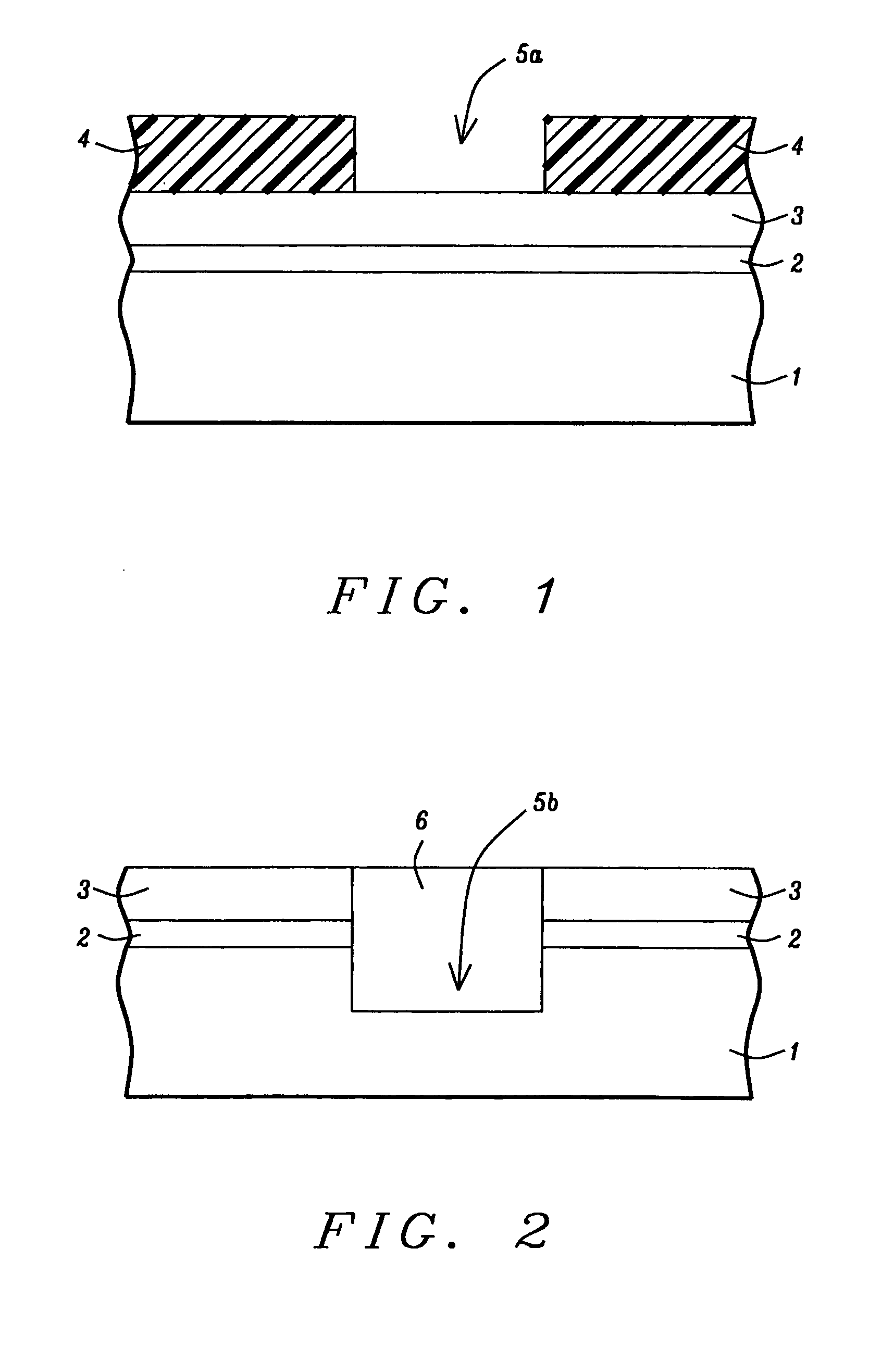
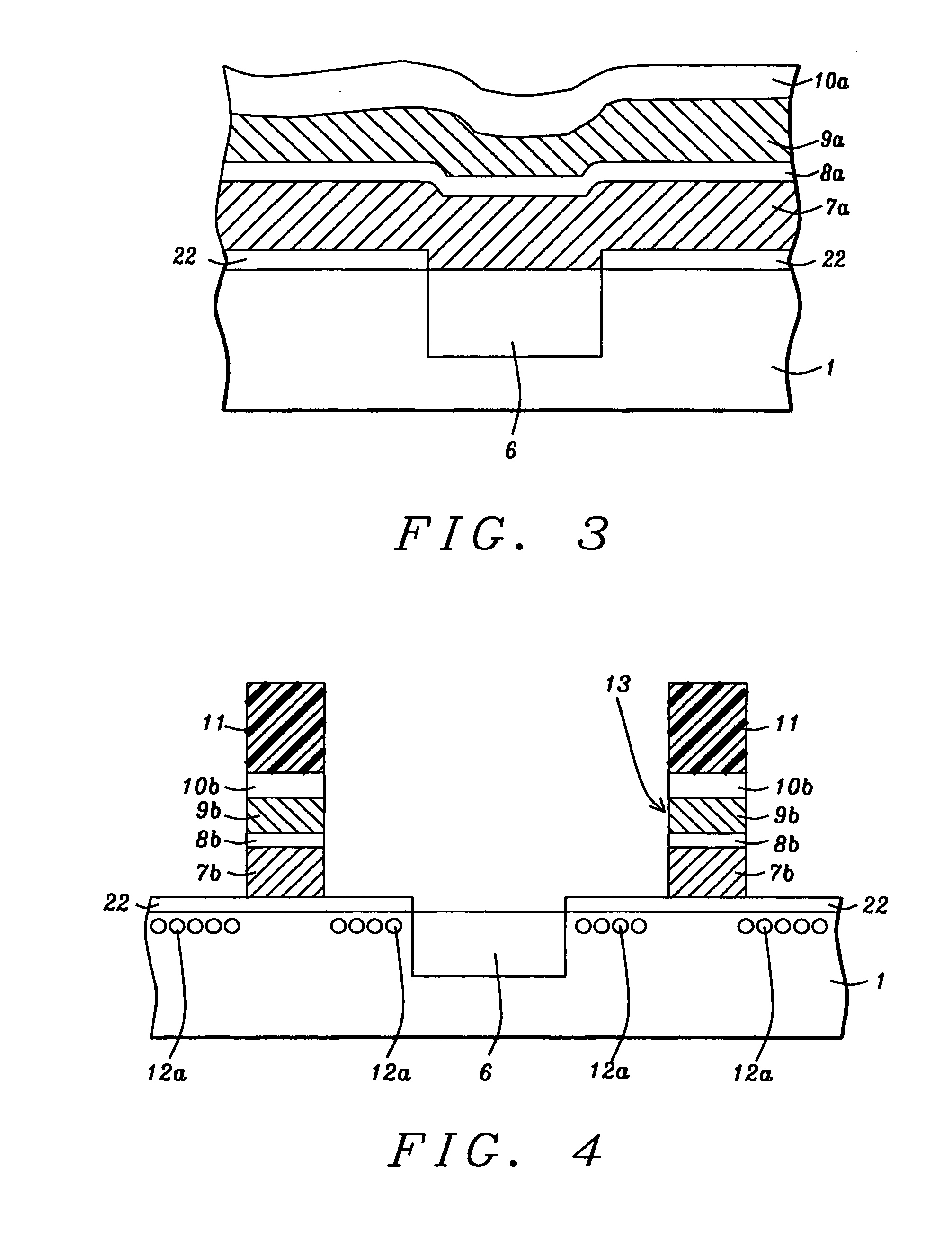
[0013]A process used to fabricate a metal oxide semiconductor (MOS) device, specifically a DRAM device, wherein implantation of group V elements wit atomic mass equal or greater than arsenic is employed to passivate defects created at or near the surface of a semiconductor substrate, defects which resulted from high density plasma etching procedures, will now be described in detail. Semiconductor substrate 1 comprised of single crystalline silicon, with a crystallographic orientation is shown schematically in FIG. 1. Insulator layer 2 comprised of silicon dioxide, is next thermally grown to a thickness between about 90 to 100 Angstroms, in an oxygen-steam ambient at a temperature between about 900 to 920° C. Silicon nitride layer 3 is next formed on insulator layer 2, via chemical vapor deposition (CVD) procedures, such as low pressure chemical vapor deposition (LPCVD), or plasma enhanced chemical vapor deposition (PECVD). Silicon nitride layer 3 is grown to a thickness between abo...


PUM


Abstract

A process for fabricating an MOS device specifically a DRAM device, featuring passivation of defects in regions of a semiconductor substrate wherein defects left unpassivated can deleteriously influence data retention time, has been developed. A high density plasma dry etching procedure used to define the DRAM conductive gate electrode can create unwanted defects in a region near the surface of uncovered portions of the semiconductor substrate during the high density plasma procedure over etch cycle. Implantation of a group V element such as arsenic can be used to passivate the unwanted plasma etch defects, thus reducing the risk of defect related device leakage phenomena. However to insure the group V implanted species remain at or near the semiconductor surface for optimum defect passivation, the group V element implantation procedure is performed after all high temperature DRAM fabrication steps, such as selective oxidation for creation of oxide spacers on the sides of the conductive gate electrode, have been completed. A slow diffusing implanted arsenic ion is the optimum candidate for passivation while faster diffusing group V elements such as phosphorous are not as attractive for defect passivation.

Description

BACKGROUND OF THE INVENTION[0001](1) Field of the Invention[0002]The present invention relates to methods of fabricating semiconductor devices, and more specifically to a method for passivating defects on a semiconductor substrate wherein the defects are a result of plasma etching procedures.[0003](2) Description of Prior Art[0004]Dynamic Random Access Memory (DRAM) devices require specific elements to retain induced charge for significant periods of DRAM operation. The ability of the DRAM elements to retain charge, or data retention time, is strongly influenced by the perfection or defect density of the portion of semiconductor substrate used for DRAM stored charge elements. Unwanted defects in portions of the semiconductor substrate will result in charge leakage, low retention time, and thus poor device yield and performance. Unfortunately several semiconductor device fabrication procedures can create defects in semiconductor substrates thus challenging the ability to fabricate ef...

Claims


Application Information

Patent Timeline
Patent Type & Authority Applications(United States)
IPC IPC(8): H01L21/02
CPCH01L27/10873H01L21/26513H10B12/05
Inventor KUMAR, ARVINDCHOW, KEEN WAHDATTA, DEVESH KUMARKRISHNAN, SUBRAMANIAN
Owner TECH SEMICON SINGAPORE PTE
Why Eureka
Try Eureka