Coaxial light-guide system consisting of coaxial light-guide fiber basing its refractive index profiles on radii and with its coaxial both semiconductor light sources and semiconductor detectors

a light-guide fiber and coaxial technology, applied in the field of communication optical fiber, to achieve the effect of reducing transmission loss, saving collapse process cost, and increasing bandwidth

Inactive Publication Date: 2008-06-19
YANG CHUN CHU
View PDF7 Cites 16 Cited by
  • Summary
  • Abstract
  • Description
  • Claims
  • Application Information

AI Technical Summary

Benefits of technology

[0051]As a conclusion, the invention, after repositions the light guide refractive index profile on the radius in the optical fiber, can eliminate the disadvantages of the prior optical fiber that has the refractive index profile done on the diameter. The shortcomings occurred to the light source and photodiode of the prior techniques also are overcome. In addition, the invention also can accomplish the following objects:
[0052]1. The problem of center-dip in the refractive index profile occurred by adopting the MCVD, PCVD and OVD methods are eliminated, and various types of high quality optical fibers with desired refractive index profile can be fabricated by employing the MCVD, PCVD and OVD methods to enable light to propagate in the optical fiber according to a selected path.
[0053]2. The preform tube formed by inside deposition can go through quality control process in advance and fibers can be drawn, thus the cost of collapse process can be saved and transmission loss can be reduced. Bandwidth also increases. By omitting collapse process of the preform tube a great amount of energy can be saved. Coupled with direct fiber drawing, contamination of water molecules during the traditional hours of collapse process can be prevented. Moreover, during collapsing performed horizontally on a glass lathe the preform often is deformed due to alignment problem of chucks at two sides of the lathe and dislocation at high temperature and spinning operation. Such deformation caused by operation often reduces the genuine circularity of the internal structure of the solid preform and increases the concentricity of the core. This impairs transmission characteristics and affects quality. The coaxial optical fiber of the invention has the preform tube going through quality control and fibers can be drawn directly and by means of vertical machines, energy waste occurred to solidifying the core of the preform is reduced. Manufacturing time is shorter and the required investment on horizontal collapsing machinery is less. Moreover, the light guide core is not contaminated. Hence high quality products can be obtained.
[0054]3. Optical wave energy that mainly concentrates to pass through the refractive index profile center is moved to the middle portion of the entire radii, and the single-mode optical fiber has the effective optical flux ratio increased by 16.5 times, utilization of the expensive semiconductor material also is higher, thus manufacturing cost is lower.
[0055]4. By moving the refractive index profile center that the optical wave main energy passing from prior axial tiny core to the middle portion of entire the radii, total optical flux increases by 16.5 times. Such an approach combines the double advantages of both the traditional single-mode optical fiber and multimode optical fiber. The invention, not only can reduce connection loss, also does not need to adopt the graded index multimode optical fiber which is more complex and expensive to fabricate. The optical fiber of the invention can be fabricated simpler and mate snugly the light source and photodiode to achieve optimal power utilization. In addition, a single-mode optical fiber made from silicon can be selected to 5obtain zero dispersion at wavelength 1300 nm. All the desirable factors set forth can be combined to increase communication distance or reduce the costs of light source and operation so that more applications of optical communication can be developed and adopted, especially Fiber-To-The-Home broadband applications. This ultimately contributes smoother flow of information and knowledge sharing for mankind.
[0056]5. The coaxial optical fiber, coaxial light source and coaxial photodiode of the invention can be coupled to form a desired integrated combination. A novel coaxial light guide system is created. It makes utilization of light guide materials more effective. The valuable laser energy can be more efficiently deployed to transmit rare photons to be detected at a farther remote end.

Problems solved by technology

1. The prior optical fiber fabricated through the methods of MCVD, PCVD and OVD cannot form a desired refractive index profile center. Around the refractive index profile center where the refractive index is highest deposition has been finished for a number of layers, but the axis portion is still hollow. The hollow portion is gradually collapsed under high temperature to become a solid core. During this process the deposited layers are not shielded or protected. A great amount of the doped material GeO2 which aims to increase the refractive index evaporates. As a result the refractive index is lower than the expected level. And depressed is formed on the refractive index profile center, thus light guide in the center is not desirable.
2. Exposition of the inner layer of the preform tube makes prior quality control not possible and results in waste of collapse process cost. To fabricate the prior optical fiber preform through the methods of MCVD and PCVD, when the deposition has been finished for a number of layers around the refractive index profile center where refractive index is highest, the axis portion where the core is intended to be formed is still hollow. Before the hollow portion is collapsed to become a solid preform, to move it to the ordinary environment to do quality control and inspect the refractive index is difficult unless a very strict temperature protection environment is provided. This is especially true for MCVD and PCVD methods in which the hollow portion of the preform has a larger internal diameter that is not protected. A direct collapse process has to be adopted to prevent contamination of the most important core and absorption loss of OH ions, and difference of internal and external stress that could cause crack. Due to the inner layer of the preform tube is exposed and the direct collapse process has to be adopted, and the collapse process has been performed for a number of hours, to prevent depressed and deformation caused by impact of high temperature gas while the exterior of the preform tube is heated, gas must be injected to keep a constant internal pressure to maintain the genuine circle of the preform and the drawn optical fiber. This internal gas flow for a prolonged period of time incurs other problems such as leakage of gas and moisture content of the gas injection system. As a result OH content in the core of the optical fiber often increases and loss also is higher.
3. The single-mode optical fiber which provides maximum bandwidth has too small of core which is difficult to connect. It also results in a lower utilization of the light guide material and waste of the highly pure material resources. It is not environmental friendly and does not fully utilize the fine and pure material. The single-mode optical fiber adopted at present for optical communication that provides maximum bandwidth has a very small core, with a diameter about 10 μm. Its light guide core area is less than 1% of the cross section of the optical fiber. 99% of the cross section provides support. Hence the ratio (A) of effective utilization area in an unit area is too low and result in waste of fine and pure material resources. For instance, for a single-mode optical fiber with an outer diameter of 125 μμm and the core diameter of 10 μm, the effective area utilization ratio of the light guide material A=52π / 62.52π×100%=0.64%. It is too low and does not fully utilize the available capability of the single-mode optical wave propagation to achieve communication purpose.

Method used


Image

  • Coaxial light-guide system consisting of coaxial light-guide fiber basing its refractive index profiles on radii and with its coaxial both semiconductor light sources and semiconductor detectors
  • Coaxial light-guide system consisting of coaxial light-guide fiber basing its refractive index profiles on radii and with its coaxial both semiconductor light sources and semiconductor detectors
  • Coaxial light-guide system consisting of coaxial light-guide fiber basing its refractive index profiles on radii and with its coaxial both semiconductor light sources and semiconductor detectors

Examples


embodiment 1

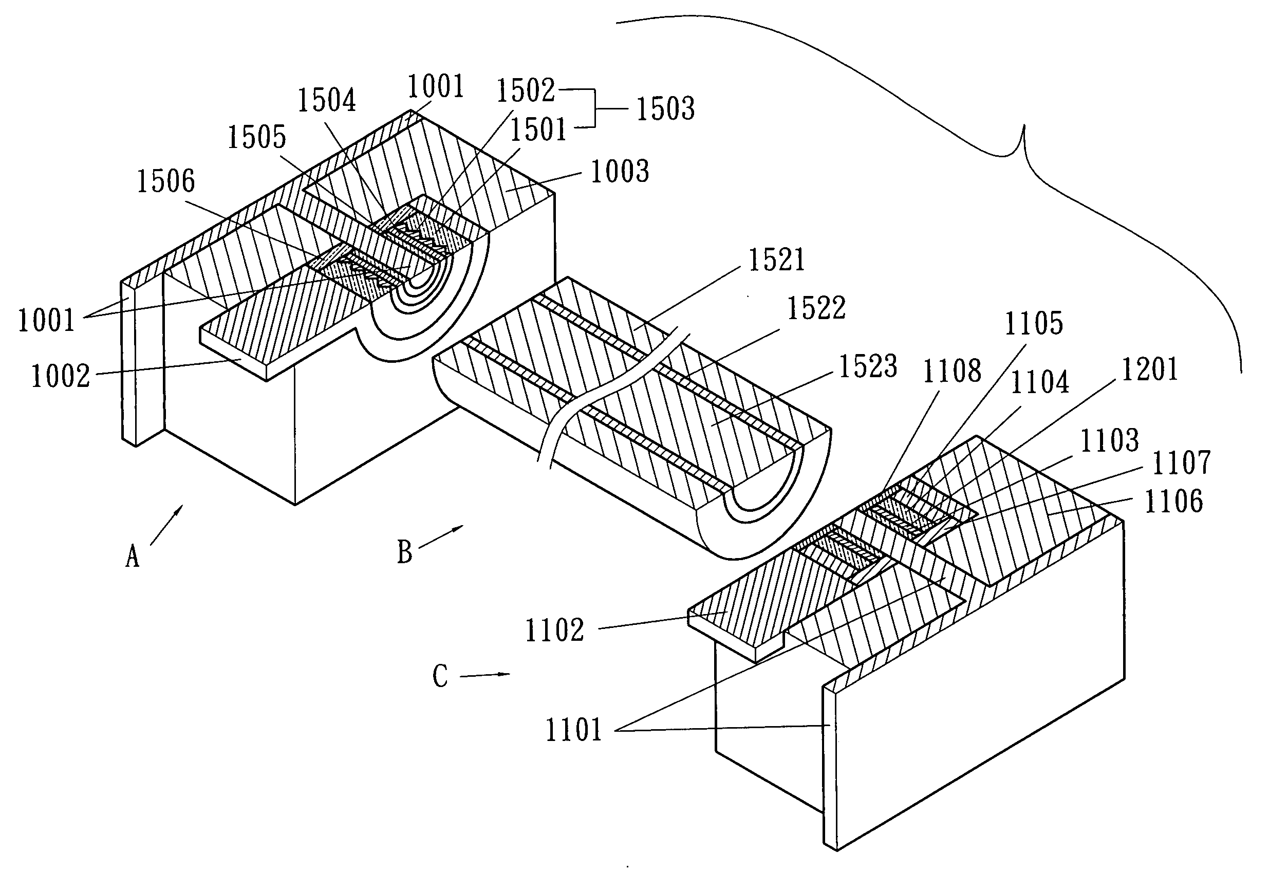
[0086]An optical fiber system consisting of a coaxial optical fiber, a coaxial light source and a coaxial photodiode that is coupled with a transceiver end is illustrated in FIG. 15. The numerals that are same as the ones of previous discussion are deemed to provide same or similar functions. The drawings are merely a simplified means to elaborate the features of the invention, and do not intend to cover all the details of actual practice nor present by actual dimensional scale. However they reflect the basic coaxial light guide principle the invention adopts.

[0087]In FIG. 15 the light source A is a coaxial semiconductor laser. It is a coaxial DFB heterostructure Distributed Feedback Bragg's laser diode shown in a fragmentary sectional view. Its structure adopts a prior planar DFB heterostructure Distributed Feedback Bragg's laser diode to coincide with natural law which the present invention intends to establish. More specifically, the DFB heterostructure laser includes a conductiv...

embodiment 2

[0097]Refer to FIG. 16 for a second embodiment of the coaxial light guide system. It is an application example co-constructed with a coaxial semiconductor transceiver on a same substrate 1602 to share a single coaxial optical fiber 801 to save another optical fiber. The prior transceiver of optical fiber has the light emitter and the photodiode which receive optical signals fabricated separately, then coupled together. As the optical fiber can transmit optical wave in both directions, in the invention with the coaxial semiconductor light transceiver co-constructed on the same substrate a lot of hardware cost can be saved. Because all of three coaxial structures are co-constructed, they can be easy stacked in an up and down manner to form various types of combinations for different applications. The transceiver has an APD photodiode at an upper layer, 1103 is a n+ semiconductor layer, 1202 is a p-type multiplication layer, 1104 is an InP intrinsic semiconductor, 1105 is a p-type semi...


PUM


Abstract

A coaxial light-guide system includes a coaxial light-guide optical fiber which is fabricated by having refractive index profile set on radii. Thus the coaxial circular outer-cladding and the axial inter-cladding have the same refractive index. The light guide refractive index profile center is moved from the axis to the entire radii of the optical fiber. Light propagates between the axial inter-cladding and the coaxial circular outer-cladding. Such a new positioning prevents center-dip in the refractive index profile that occurs to the prior optical fiber after fabrication is finished. The coaxial single-mode optical fiber of the invention has a greater optical flux than the prior optical fiber, and can increase communication distance. Coupled with a coaxial light source and photodiode of the invention that have an coaxial inner and outer conductors to supply electric power and a plurality of annular semiconductor layers interposed therebetween, energy waste caused by prior edge-emitting elliptic light source injecting in a circular core can be eliminated.

Description

FIELD OF THE INVENTION[0001]The present invention relates to a communication optical fiber and particularly to a coaxial light guide system equipped with a light source and a photodiode.BACKGROUND OF THE INVENTION[0002]Human being discovered glass about 2500 years ago, and learned to draw fibers from the glass until at Roman time. In 1950 medical field tried to bind bare glass fibers into a bundle to transmit images to be used as an endoscope. But light leakage was too much and images could not be clearly transmitted. It was mainly because the bare glass fibers did not have a desired purity and the external air that has a lower refractive index serves as a total reflective layer. In 1956 Dr. Narinder Singh Kapany first coined the term “fiber optical”. By wrapping more precisely a layer of glass material of a lower refractive index around a bare glass fiber as an outer shell total reflection was controlled more effectively and light leakage was prevented. As a result the optical fibe...

Claims


Application Information

Patent Timeline
Patent Type & Authority Applications(United States)
IPC IPC(8): H01L33/00G02B6/036H01L31/00G02B6/028H01L31/10H01L31/107H01S5/12
CPCG02B6/03611H01L31/03046H01L31/07G02B6/4246Y02E10/50G02B6/4203H01L31/105
Inventor YANG, CHUN-CHU
Owner YANG CHUN CHU
Why Eureka
Try Eureka