Method and Structure for Optimizing Yield of 3-D Chip Manufacture

a technology of 3-d chips and manufacturing methods, applied in the direction of electrical equipment, semiconductor devices, semiconductor/solid-state device details, etc., can solve the problems of limiting the performance gain of single chips and multi-chip packages, affecting the availability of connections to the outside package, and affecting the efficiency of 3-d chip manufacturing, etc., to achieve the effect of reducing the aspect ratio of the via, reducing the frequency of good-die-to-good-die bonding, and reducing the cos

Active Publication Date: 2008-06-19
INT BUSINESS MASCH CORP
View PDF2 Cites 182 Cited by
  • Summary
  • Abstract
  • Description
  • Claims
  • Application Information

AI Technical Summary

Benefits of technology

[0015]It is another object of the present invention to maximize the frequency of good-die-to-good-die bonding in a 3-D chip integration process consistent with chip thinning.
[0016]The method of the present invention involves several steps, beginning with forming at least two complimentary chips on separate device wafers. These chips are designed complementarily such that they can be interconnected by stacking to form a chip stack. If a chip stack is comprised of two separate chips of types A and B, then all chips of type A are formed on device wafers of type X, and all chips of type B are formed on device wafers of type Y. Instead of typical C4 or solder bump metallurgy, thin metal capture pads are deposited on both wafers. These pads can be made of Cu, Au, Al, or Sn. The preferred metal is Sn, due to its low cost, resistance to oxidation and ease of plating. Additionally, Sn is preferred for the pads that are tested and then removed, whereas Cu is preferred for the pads that are bonded together. In the preferred embodiment, pads that will be used for testing and subsequently removed are made of Sn, and pads that will be bonded together are made of Cu. For reasons discussed below, the thickness of the final capture pads is preferably about 10 microns. Both wafers are then tested to determine and map the good chip sites.
[0017]After mapping good chip sites, one device wafer is subjected to a thinning process. In the previous example, if a chip of type A is to be thinned, then device wafers of type X are subjected to the thinning process. Thinning the device wafer consists of attaching a handle wafer to the top side of the device wafer. The bottom side of the device wafer is then ground, polished, etched or the like until the wafer is approximately 50 microns thick. Vias are then etched into the device wafer and filled with metal to provide vertical connection between metal interconnect lines on respective stacked chips. Thinning the chip results in a large decrease in aspect ratio of the vias, thereby reducing the difficulty of reliably filling vias with metal.

Problems solved by technology

However, while functionality and manufacturing economics may increase from increased integration density, there is a limit to performance gain with single chips and multi-chip packages due to signal propagation increases with increased connection length.
Some of these limitations may be overcome with 3-D geometries but may also suffer limitations due to interchip connections in known chip stacking technologies.
Known chip stacking technologies and their problems include 1) connection density versus yield, and 2) number of connections between chips, especially using edge bonding.
Another example is the so-called “mother / daughter” chip structure, which has been used to provide a large number of inputs / outputs (I / Os) between two chips, although it can create limitations on the available area to make connections to the outside package.
Thinned chips can function at higher speeds and consequently increased heat dissipation, since the insulating silicon between the device and thermal management material is reduced.
In practice, however, it is very difficult to implement a truly high-performance system because of different fabrication processes and lower manufacturing yields for the logic and memory circuits, and different preferred technologies for respective functional sections such as processors, gate arrays, memories, distributed power regulators, connectors and the like.
For example, integrating functions onto a single chip generally require compromise of the performance of the logic and the performance / density of the memory.
Further, the chips often become very large, and the yield of fully functional chips decreases.
One problem associated with the background art, however, involves the general trend of device yield decreasing as device complexity, integration density, or chip size, increases.
This trend can be attributed to the fact that for the same quality of semiconductor, any defect existing in a larger chip results in an overall greater area waste than is the case with smaller chip wafers.
Thus as chip size increases, the cost of manufacturing due to yield degradation becomes excessive.
The major disadvantage of this method is the difficulty in controlling the amount of soldering solution that contacts the stacked chips.
Additionally, densely packed leads often results in short-circuiting.
The disadvantage to this approach is that any need for repair of the module after package fabrication would cause the entire module to be rejected.
One shortcoming of these conventional contact fabrication processes is that time and materials are wasted in forming the contacts on defective and substandard components.
Additionally, pressure joining processes tend to crush or compress C4s, resulting in shorting of C4 interconnects.
Thus, because of the height of these connections relative to the chip, and the ease at which these connections can be damaged, another limitation is that pressure and mechanical strain must be limited while integrating chips containing these types of connections.
Also, C4s will melt at high temperatures, which restrains subsequent processing conditions and operating conditions.
When a via is drilled through a majority of the wafer thickness of a chip, the aspect ratio is very large, often 100:1 or more, particularly at known and foreseeable minimum feature sizes, making it difficult to fill the via with a seed metal and subsequently deposited metal to reliably and repeatably provide vertical connection between stacked up interconnect metal lines.
However, thinned chips lack structural integrity and become difficult to handle for further processing.
In this regard, an additional drawback experienced in the background art of forming stacked chips is the possibility of bonding a good chip site of one wafer to a bad chip site on another wafer.
Bonding a defective chip to a good chip, at best, causes waste of the good chip.
Such bonding may further compromise the yield because a thinned chip cannot generally be released from a chip to which it is bonded without sustaining irreparable damage.
The process of forming effective chip stacks yields functional devices only if both sites are working correctly, and there is currently no method to increase the frequency of bonding good chip sites to good chip sites, thereby increasing the yield of good, functional chip stacks.
Further, current methods of testing semiconductor devices for functional chips requires subjecting each chip to the testing method, resulting in increased fabrication cost and time.

Method used


Image

  • Method and Structure for Optimizing Yield of 3-D Chip Manufacture
  • Method and Structure for Optimizing Yield of 3-D Chip Manufacture
  • Method and Structure for Optimizing Yield of 3-D Chip Manufacture

Examples


Embodiment Construction

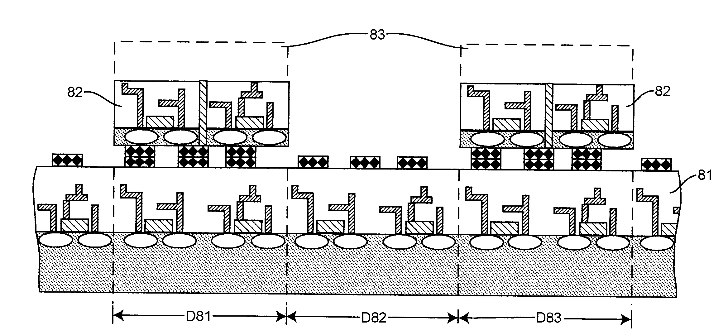
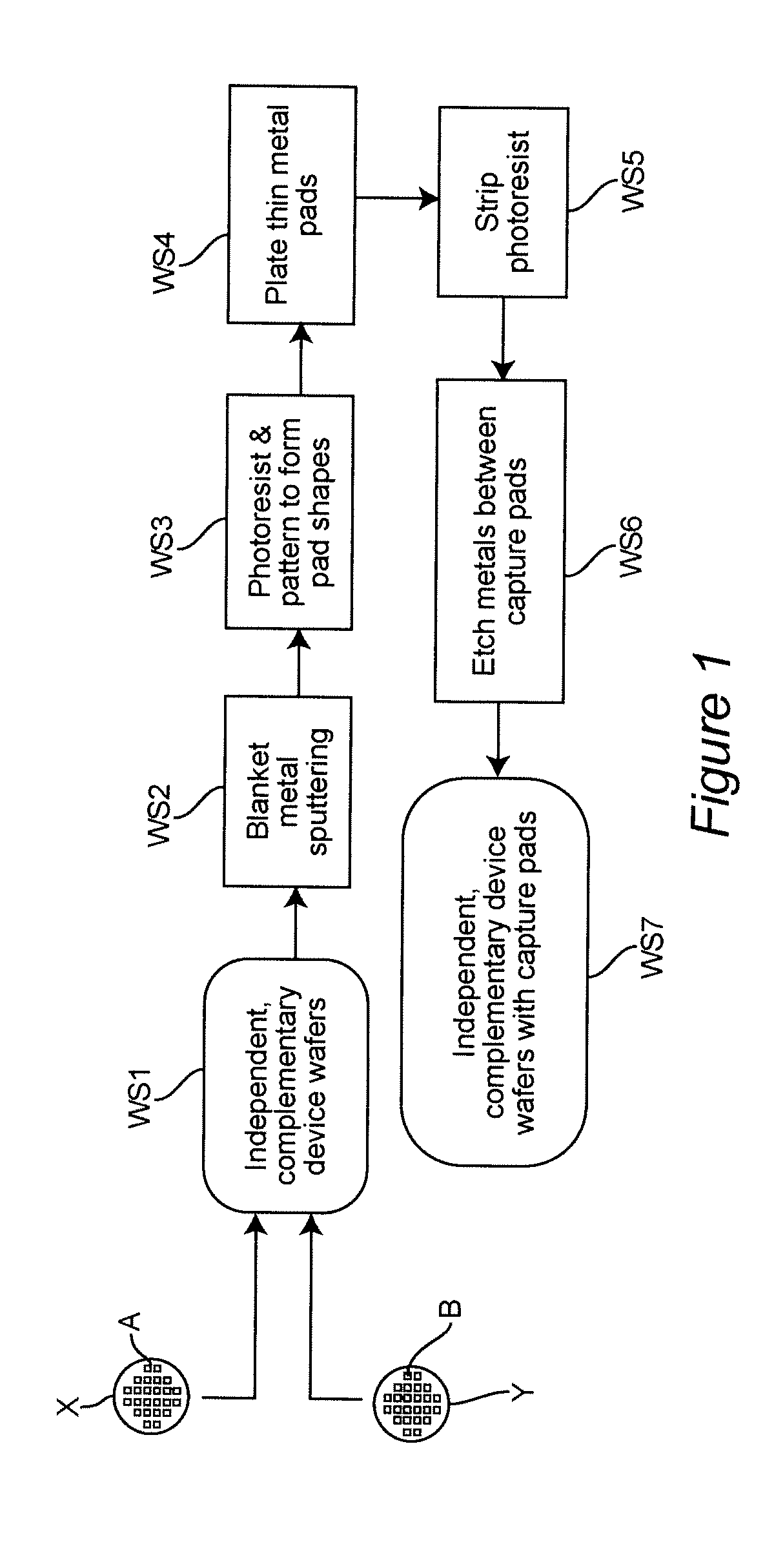
[0028]FIGS. 1 through 4c illustrate a fabrication process for a 3-D integrated chip according to a preferred embodiment of the invention. Referring to FIG. 1, the fabrication process begins with the process of forming capture pads on at least two independent device wafers X and Y already having a plurality of chips types A and B respectively formed thereon in step WS1. Chips A and B are designed such that they are complementary to one another in layout so that they may be interconnected by a 3-D integration process to form a chip stack. Blanket metals are applied to the top side of the wafers by a sputtering process in step WS2. The blanket metal layer improves the adhesion of the pads, and may consist of Cr, Cu, Ni, Ta, and various combinations of Ti, and may be in plural layers at various thicknesses. Preferably, the blanket metal layer is TiW (10 / 90) at 1650 Å, CrCu (50 / 50) at 1800 Å, and Cu at 4300 Å. Photoresist is applied to the surface and patterned in accordance with desired...


PUM


Abstract

The process begins with separate device wafers having complimentary chips. Thin metal capture pads, having a preferred thickness of about 10 microns so that substantial pressure may be applied during processing without damaging capture pads, are deposited on both device wafers, which are then tested and mapped for good chip sites. A handle wafer is attached to one device wafer, which can then be thinned to improve via etching and filling. Capture pads are removed and replaced after thinning. The device wafer with handle wafer is diced, and good chips with attached portions of the diced handle wafer are positioned and bonded to the good chip sites of the other device wafer, and the handle wafer portions are removed. The device wafer having known good 3-D chips then undergoes final processing.

Description

BACKGROUND OF THE INVENTION[0001]1. Field of the Invention[0002]The present invention generally relates to a three-dimensional (3-D) chip integration process and structure, and, more specifically, relates to a method for optimizing the yield of a three-dimensional chip integration process and 3-D chips upon completion of the integration process.[0003]2. Description of Related Art[0004]This invention relates to 3-D semiconductor devices built with potentially different technologies fabricated on separate wafers, diced, and then connected together by mounting one of the dies on the other. These devices, referred to as 3-D integrated circuits (ICs), have the potential for enabling circuit performance enhancements required to meet the aggressive performance targets of future technology. These circuits contain multiple layers of active devices with vertical interconnections between the layers. In a 3-D IC, each transistor can theoretically access a greater number of nearest neighbors tha...

Claims


Application Information

Patent Timeline
Patent Type & Authority Applications(United States)
IPC IPC(8): H01L23/488
CPCH01L21/8221H01L2224/13H01L27/0688
Inventor DEMULDER, EDWARD M.KNICKERBOCKER, SARAH H.SHAPIRO, MICHAEL J.YOUNG, ALBERT M.
Owner INT BUSINESS MASCH CORP
Why Eureka
Try Eureka