Integrated dram process/structure using contact pillars

a contact pillar and process technology, applied in the field of semiconductor memory devices, can solve the problems of reducing the cross-sectional area of single-event upset, limiting process margins such as alignment tolerance, and personal devices requiring more computational power and on-chip memory, etc., to achieve the greatest capacitance density, improve the structural strength of the cell, and reduce the effect of single-event ups

Inactive Publication Date: 2008-06-26
TEXAS INSTR INC
View PDF24 Cites 6 Cited by
  • Summary
  • Abstract
  • Description
  • Claims
  • Application Information

AI Technical Summary

Benefits of technology

[0025]In some variations of the present invention, the cells have a portion of the contact pillar structure of the capacitor plate which extends into a region of the PMD that is not removed. This improves structural strength of the cell during processing. Of these variations, the cell with contact pillars in the storage plate has the greatest capacitance density (capacitance per unit foot-print area).
[0026]Single-event upsets (SEUs) are random errors in semiconductor memory devices, which can cause a loss of data. SEUs are caused by passage of energetic charged particles through sensitive regions of a chip. Beneficially, the single-event upset cross-section is reduced by having the contact pillar structures extend over field, effectively shielding the active areas of the substrate, thus reducing random errors and the loss of data.
[0027]A further object of the present invention is to provide a method for fabricating a capacitor under bit line memory cell within the PMD layer utilizing several self-aligning steps, while performing these steps within the simple standard logic process.
[0028]Yet a further object of the present invention is to provide a DRAM cell with a three-dimensional capacitor structure utilizing contact pillar structures embedded within the PMD layer having reduced complexity and thus reduced defect rate, increased ease of manufacture, and reduced manufacturing cost.
[0029]A simple memory structure and method utilizing a three-dimensional capacitor formed substantially within the thick PMD layer provides a high density CUB type DRAM memory cell, which has memory and logic functions integrated onto the same semiconductor chip, thereby permitting the use of the simpler standard logic process with a minimum of process steps, yet has the high density benefits of the DRAM process.

Problems solved by technology

In addition to being smaller and more portable, personal devices are requiring more computational power and on-chip memory.
However, as the cell area decreases, process margins such as alignment tolerance have become limiting factors for developing a simple cost effective high density DRAM memory cell.
A characteristic of a DRAM memory is that a read operation is destructive in some applications.
Thus, simply adding the standard DRAM process to the simpler standard logic process would be too expensive, both in terms of development and production.
Additionally, as memory cell density increases, there is a continuing challenge to maintain sufficiently high storage capacitance despite decreasing cell area.
Several trench capacitor cells have had process problems, particularly where increases in cell density has pressed the access transistor alongside the trench capacitor.
Some of the process problems presented by these prior art approaches include: the epi process from the contact hole being barely controllable; the gate dielectric grown from the gate (rather than the channel) causing a potential reliability problem; alignment tolerances between contact holes; and word lines that are patterned before the contact process.
In addition, these approaches have the tendency of decreasing process margins more than conventional processes.
These additional process steps have a great impact on manufacturing costs and capitol equipment costs particularly where they are associated with added photolithographic equipment and more complex photo processing.
Defect density inevitably increases with each additional photomasking layer and compromises yield and reliability.
Thus, conventional combinations of a standard DRAM process with the simpler standard logic process have been too expensive for the applications considered.
Also, conventional prior art COB type DRAM cells integrated into the standard logic process are generally limited to the relatively thin IMD (inter-metal dielectric) layers, by comparison to some other layers under the bit line such as the PMD layer or the substrate.
This may not be a problem when planar capacitors are used in the DRAM, consuming large areas of semiconductor but when three-dimensional capacitors are to be integrated into the IMD layers, depth issues become paramount.

Method used


Image

  • Integrated dram process/structure using contact pillars
  • Integrated dram process/structure using contact pillars
  • Integrated dram process/structure using contact pillars

Examples


Embodiment Construction

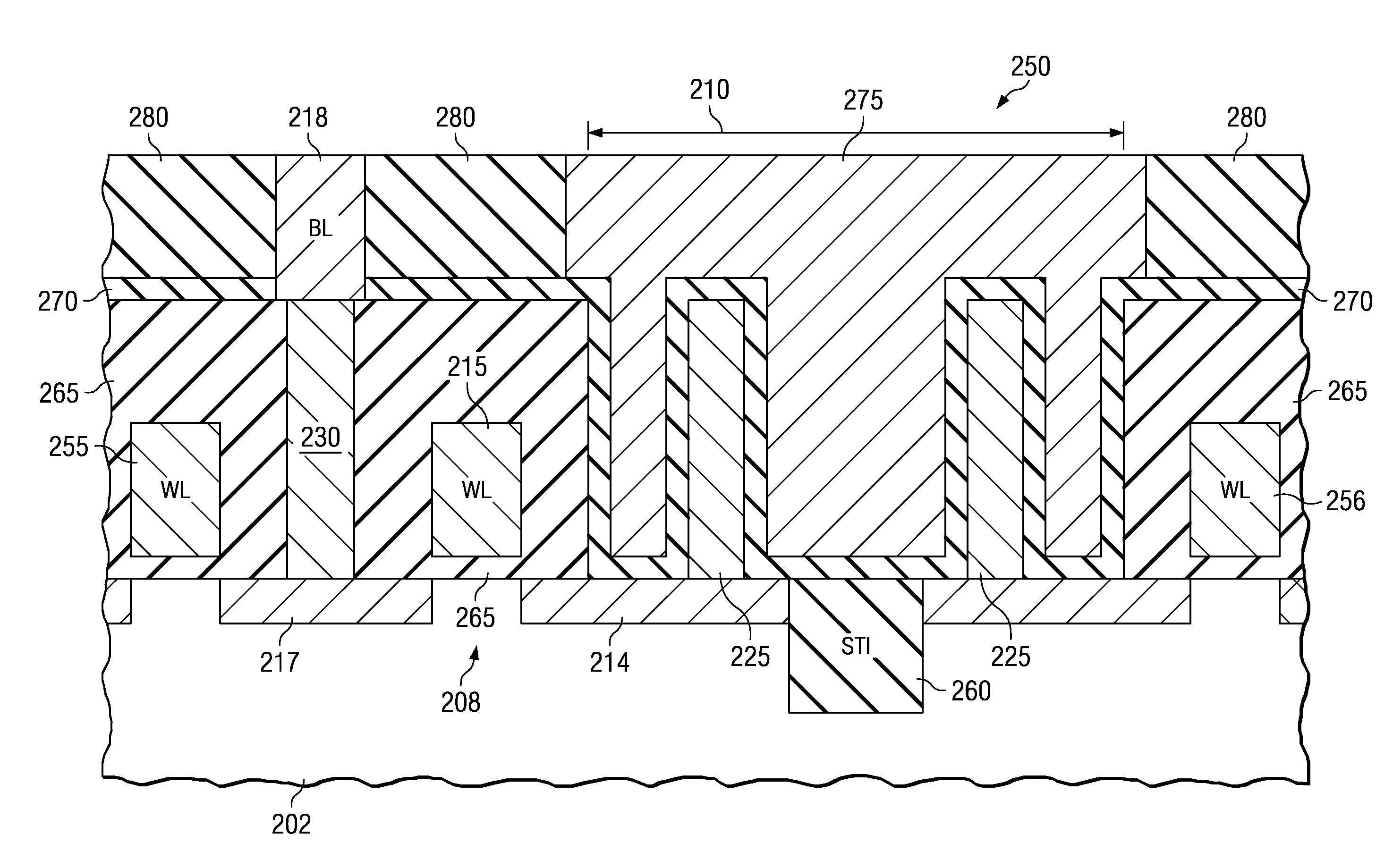
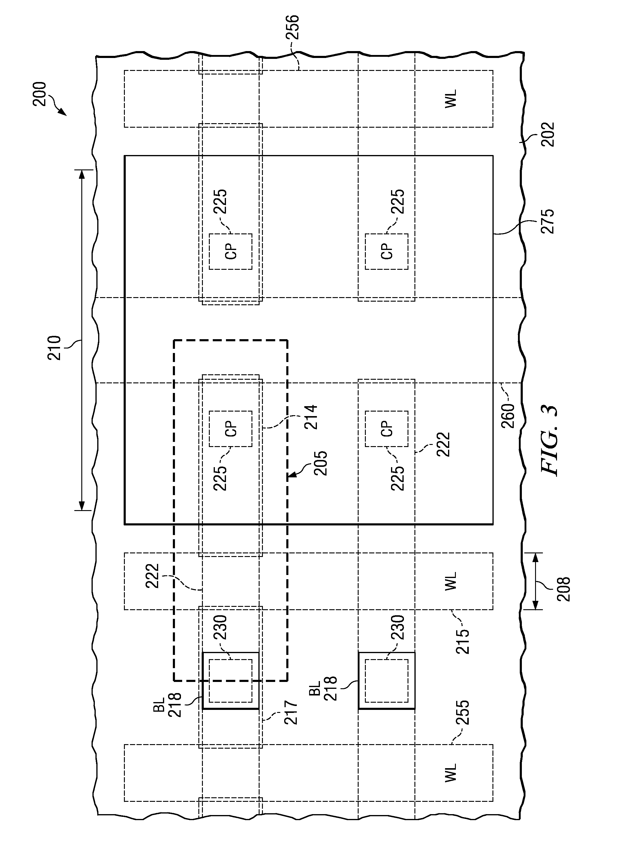
[0051]The present invention will now be described with reference to the drawings, wherein like reference numerals are used to refer to like elements throughout. The invention is directed to an embedded DRAM (eDRAM) memory device utilizing a three dimensional capacitor under the bit line (CUB) memory cell array architecture, which is believed to be applicable to a variety of memory applications. In particular, the device structure provides a system and method of forming a high density DRAM memory cell using simple standard logic type processes. The memory cell of the present invention uses several variations of a contact pillar structure comprising a contact conductive material used as a first capacitor plate formed within a trench within a first insulating layer (e.g., a PMD layer). A capacitor dielectric layer comprising, for example, a capacitor dielectric material such as Ta2O5, TiO2, or BST then covers the contact pillar structures and the trench to insulate the first capacitor ...


PUM


Abstract

A capacitor under bitline DRAM memory cell and method for its fabrication provides a high density memory cell with the capacitor formed in the PMD layer. The memory cell utilizes several variations of storage contact pillar structures as, for example, a storage plate of the memory cell capacitor formed within a trench in the PMD layer. This capacitor plate structure is overlaid with a capacitor dielectric layer which is overlaid with another conductive layer, for example, the M1 layer to form the other capacitor plate. An access transistor formed between substrate active regions and a word line, is in electrical communication with a bit line contact, the storage contact capacitor plate, and the word line respectively. The high density memory cell benefits from the simple standard processes common to logic processes, and in one embodiment requiring only one additional masking step.

Description

[0001]This application is a division of U.S. application Ser. No. 10 / 664,547 filed Sep. 19, 2003 which is a division of U.S. application Ser. No. 10 / 180,140 filed Jun. 26, 2002 now U.S. Pat. No. 6,710,391, issued Mar. 23, 2004 the entire disclosures of all of which are hereby incorporated by reference.TECHNICAL FIELD OF INVENTION[0002]The present invention relates generally to semiconductor memory devices and their manufacture, and more particularly to capacitor under bitline DRAM memory cells and methods for fabricating such structures and cells providing benefits relating to increased circuit density and processing simplicity.BACKGROUND OF THE INVENTION[0003]Several trends exist presently in the semiconductor device fabrication industry and the electronics industry. Devices are continually getting smaller and requiring less power. A reason for these trends is that more personal devices are being fabricated which are relatively small and portable, thereby relying on a small battery...

Claims


Application Information

Patent Timeline
Patent Type & Authority Applications(United States)
IPC IPC(8): H01L27/00H01L21/02H01L21/8242H01L27/108H01L29/76H01L29/94H01L31/119
CPCH01L27/10811H01L27/10817H01L28/91H01L27/10855H01L27/10852H10B12/312H10B12/318H10B12/033H10B12/0335
Inventor HOUSTON, THEODORE W.
Owner TEXAS INSTR INC
Why Eureka
Try Eureka