
Method for depositing an amorphous carbon film with improved density and step coverage

Inactive Publication Date: 2008-06-26
APPLIED MATERIALS INC
View PDF13 Cites 341 Cited by
  • Summary
  • Abstract
  • Description
  • Claims
  • Application Information

AI Technical Summary

Benefits of technology

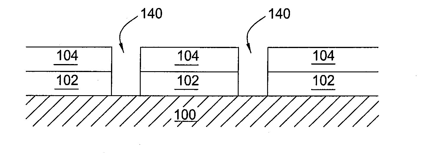
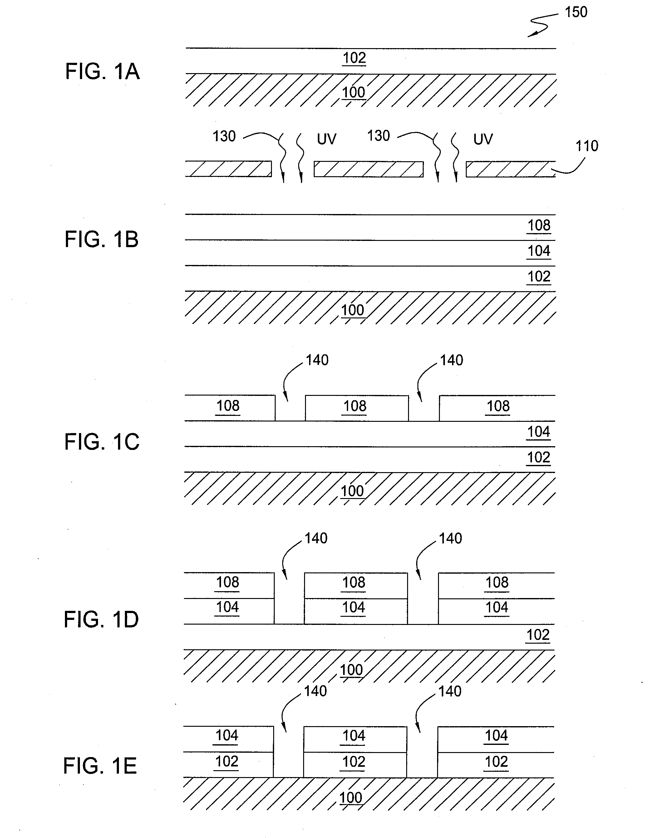
[0073]Another advantage of an argon-diluted process is that a lower temperature process may be used to produce an a-C:H layer with the desired density and transparency. Ordinarily, higher substrate temperature during deposition is the process parameter used to encourage the formation of a higher density film. Because the argon-diluted process already increases density for the reasons described above, substrate temperature may be reduced during deposition, for example to as low as about 300° C., and still produce a film of the desired density, i.e., from about 1.2 g / cc to about 1.8 g / cc. Hence, the argon-dilution process may produce a relatively high density film with an absorption coefficient as low as about 0.09. Further, lower processing temperatures are generally desirable for all substrates since this lowers the thermal budget of the process, protecting devices formed thereon from dopant migration.

Problems solved by technology

Integrated circuits have evolved into complex devices that can include millions of transistors, capacitors and resistors on a single chip.
Producing devices having low-k materials with little or no surface defects or feature deformation is problematic.
Low-k dielectric materials are often porous and susceptible to being scratched or damaged during subsequent process steps, thus increasing the likelihood of defects being formed on the substrate surface.
Low-k materials are often brittle and may deform under conventional polishing processes, such as chemical mechanical polishing (CMP).
Such device structures, therefore, cannot be patterned using a silicon dioxide or silicon nitride hardmask as an etch mask, since there will be little or no etch selectivity between the hardmask and the material thereunder, i.e., removal of the hardmask will result in unacceptable damage to underlying layers.
The lack of complete coverage of sidewalls 204 by non-conformal amorphous carbon layer 202 may also lead to photoresist poisoning of the material under non-conformal carbon layer 202, which is known to damage electronic devices.
For example, if, during the formation of a hardmask, a large numbers of particles that can contaminate the substrate are generated, or the devices formed on the substrate are excessively heated, the resulting problems can easily outweigh any benefits.

Method used


Image

  • Method for depositing an amorphous carbon film with improved density and step coverage
  • Method for depositing an amorphous carbon film with improved density and step coverage
  • Method for depositing an amorphous carbon film with improved density and step coverage

Examples


Embodiment Construction

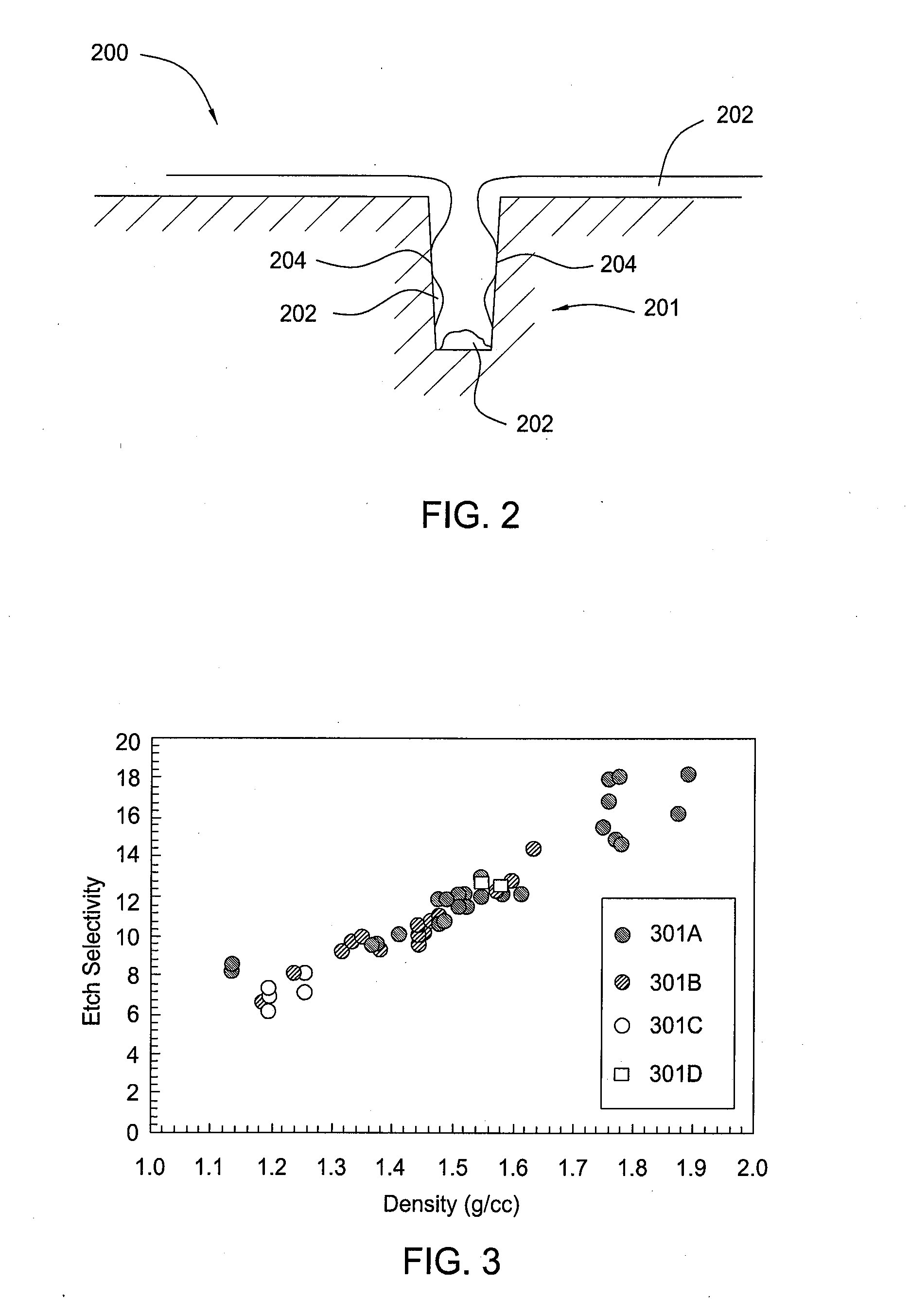
[0039]The inventors have learned that there is a strong correlation between a-C:H film density and etch selectivity regardless of the hydrocarbon source used to deposit the a-C:H film. FIG. 3 is a graph plotting the relationship between film density and etch selectivity of multiple samples of four different a-C:H films 301A-D deposited on different substrates. Etch selectivity is the factor by which an underlying material is etched compared to a given a-C:H film, i.e., an etch selectivity of 10 indicates that an underlying material is removed ten times faster than the a-C:H film. Each of films 301A-D were formed from different precursors and processing conditions. The data reveal a substantially linear correlation between the density and etch selectivity of each film regardless of the precursor. These results demonstrate that it is possible to achieve a desired etch selectivity for an a-C:H film by increasing the film density, even though the processing temperatures and precursors a...


PUM

PropertyMeasurementUnit
Temperatureaaaaaaaaaa
Timeaaaaaaaaaa
Pressureaaaaaaaaaa

Abstract

A method for depositing an amorphous carbon layer on a substrate includes the steps of positioning a substrate in a chamber, introducing a hydrocarbon source into the processing chamber, introducing a heavy noble gas into the processing chamber, and generating a plasma in the processing chamber. The heavy noble gas is selected from the group consisting of argon, krypton, xenon, and combinations thereof and the molar flow rate of the noble gas is greater than the molar flow rate of the hydrocarbon source. A post-deposition termination step may be included, wherein the flow of the hydrocarbon source and the noble gas is stopped and a plasma is maintained in the chamber for a period of time to remove particles therefrom.

Description

CROSS-REFERENCE TO RELATED APPLICATIONS[0001]This application is a continuation-in-part of co-pending U.S. patent application Ser. No. 11 / 427,324, filed Jun. 28, 2006, entitled “Method for Depositing an Amorphous Carbon Film with Improved Density and Step Coverage,” which is incorporated herein in its entirety by reference.BACKGROUND OF THE INVENTION[0002]1. Field of the Invention[0003]Embodiments of the present invention generally relate to the fabrication of integrated circuits and particularly to the deposition of an amorphous carbon layer on a semiconductor substrate.[0004]2. Description of the Related Art[0005]Integrated circuits have evolved into complex devices that can include millions of transistors, capacitors and resistors on a single chip. The evolution of chip design continually requires faster circuitry and greater circuit density. The demand for faster circuits with greater circuit densities imposes corresponding demands on the materials used to fabricate such integra...

Claims


Application Information

Patent Timeline
IPC IPC(8): H01L21/31
CPCC23C16/045C23C16/26H01L21/3146C23C16/56H01L21/31144C23C16/5096H01L21/02274H01L21/02115H01L21/02592
Inventor PADHI, DEENESHHA, HYOUNG-CHANRATHI, SUDHAWITTY, DEREK R.CHAN, CHIUPARK, SOHYUNBALASUBRAMANIAN, GANESHJANAKIRAMAN, KARTHIKSEAMONS, MARTIN JAYSIVARAMAKRISHNAN, VISWESWARENKIM, BOK HOENM'SAAD, HICHEM
Owner APPLIED MATERIALS INC
Learn More