Interconnections for flip-chip using lead-free solders and having improved reaction barrier layers

a technology of flip-chips and solders, applied in the direction of semiconductor devices, semiconductor/solid-state device details, electrical apparatus, etc., can solve the problems of limiting the extendibility of large wafers, pb-free applications, and more dense arrays

Inactive Publication Date: 2008-07-03
ULTRATECH INT INC
View PDF21 Cites 26 Cited by
  • Summary
  • Abstract
  • Description
  • Claims
  • Application Information

AI Technical Summary

Benefits of technology

[0018]It is another object of the invention to provide flip chip electrical connections that reduce the occurrence of soft errors in computer chips.
[0019]The present invention focuses on cost-effective, environmentally sound, reliable BLM for lead-free solders in C4 joints. The present invention also provides the enabling processes for fabrication of an integrated C4 structure, i.e., the selection of the BLM and the deposition and patterning processes used to produce the final BLM structure.
[0021]The elimination of lead from electronic solders is desirable because of the toxicity of lead. Lead leaching out from the electronic assembly in landfill into ground water under acid rain condition has been widely reported. The use of lead-free solders also facilitates a means of limiting the soft error rates in IC device that are caused by alpha particle emission from leaded solder.
[0024]The invention is also directed to an interconnection structure suitable for flip-chip attachment of microelectronic device chips to packages, comprising a two-layer BLM structure comprising an adhesion and a reaction barrier layer, wherein the two layer structure condenses the adhesion, reaction and wettable properties of a multilayer thin film structure into two layers, thus simplifying process steps and reducing production cost. In one example, the adhesion / barrier layer is combined with a solder wettable layer which is a metal layer readily reactive with a tin-containing lead-free solder, so that the solder wettable layer is consumed during soldering, wherein the adhesion / reaction barrier layer remains after being placed in contact with the lead free solder during soldering; and one or more lead-free solder balls are selectively situated on the solder wettable layer, the lead-free solder balls comprising tin as a predominant component doped with one or more alloying components. The adhesion / reaction barrier layer may preferably be comprised of a material selected from the group consisting of one of TiW, TiN, and Ti. The solder wettable layer may preferably be comprised of a material selected from the group consisting of Cu, Au, Pd, Ni, Co, Ru, and Sn, and their alloys. The interconnect structure may further comprise an optional third layer preferably comprised of Au or Sn, if they have not already been used in the second layer. Preferably, the lead-free solder ball is comprised of a material that substantially avoids alpha particle emission. The solder alloys having tin as a predominant component and one or more alloying components preferably selected from the group consisting of Cu, Ag, Bi, Ni, Co, Fe, and Sb.
[0025]The invention is also directed to an interconnection structure suitable for flip-chip attachment of microelectronic IC device chips to packages, comprising a three-layer BLM, an adhesion layer, a reaction barrier layer on top of the adhesion layer and a solder wettable layer, wherein the adhesion / barrier layer is between a microelectronic device and the solder wettable layer and wherein the solder wettable layer is of a composition sufficiently reactive with components of a tin-containing lead free solder, and the reaction barrier layer is substantially less-reactive with solder after being placed in contact therewith in a solder joining process; and one or more lead-free solder balls selectively situated on the solder wettable layer, whereby the lead-free solder ball substantially avoids alpha particle emission and induced soft logic errors which result therefrom.

Problems solved by technology

However, it is believed that the limit of extendibility to larger wafer sizes, more dense arrays and Pb-free applications has nearly been reached by the evaporation method.

Method used


Image

  • Interconnections for flip-chip using lead-free solders and having improved reaction barrier layers
  • Interconnections for flip-chip using lead-free solders and having improved reaction barrier layers
  • Interconnections for flip-chip using lead-free solders and having improved reaction barrier layers

Examples


example 1

ayer BLM

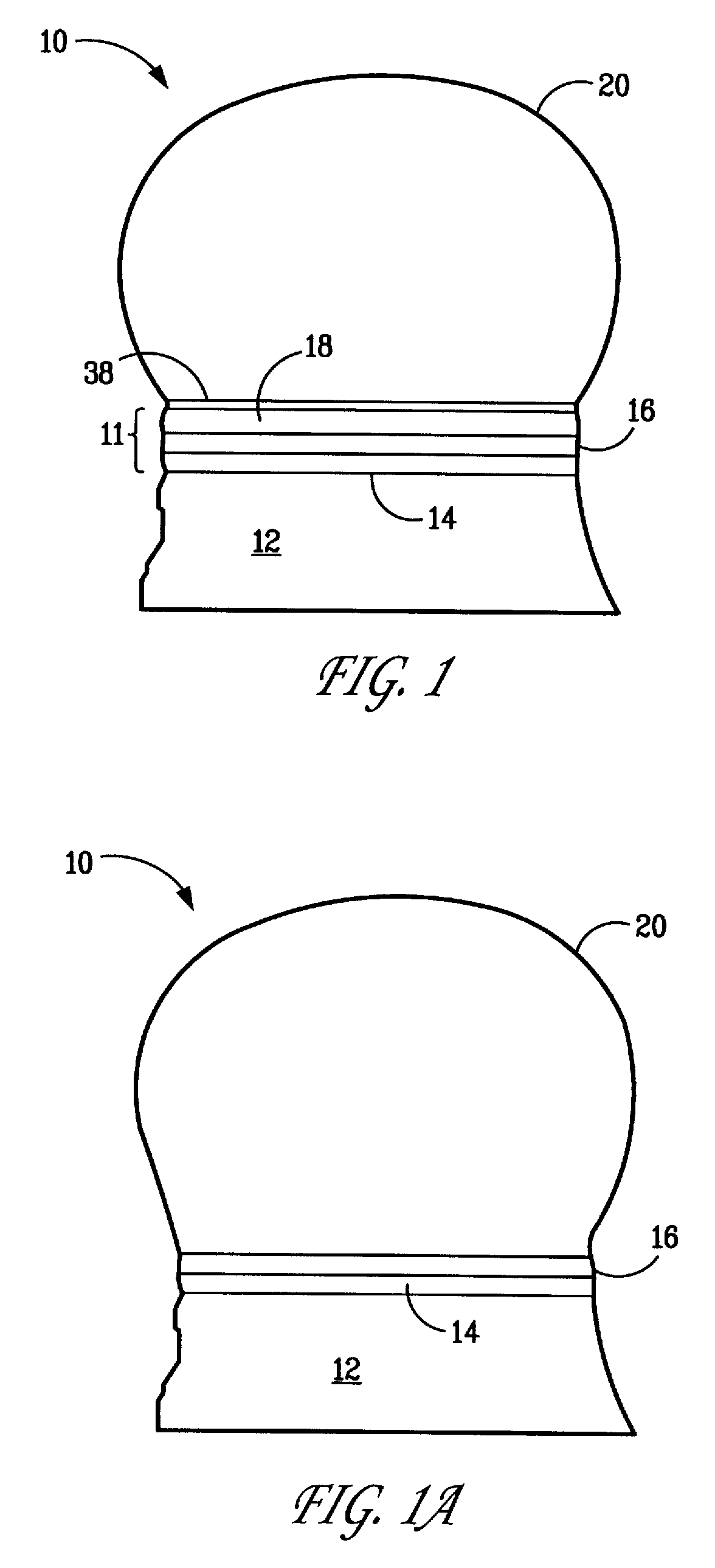
[0044]In accordance with the present invention, a preferred adhesion layer 14 is TiW or Ti, which is preferably either sputtered or evaporated, at a preferred thickness of about 100 to 5000 angstroms. The thickness of the adhesion layer 14 can vary widely as long as both good adhesion and good barrier properties are maintained. If blanket TiW is deposited and subsequently etched as the final step in forming the patterned BLM structure, 11, the film thickness should be minimized consistent with adequate performance. An alternative adhesion layer is Cr, Ta, W or their alloys at a thickness of about 100 to 5000 angstroms.

[0045]The second layer 16 is a solder reaction barrier layer, preferably typically a few thousand angstroms to several microns in thickness, deposited preferably by sputtering, evaporation or plating. Since the high tin content Pb-free solders are highly reactive than the eutectic Pb-rich Pb—Sn solder, a thick reaction barrier layer is needed to survive multipl...

example 2

yer BLM

[0051]In this example, the first layer is preferably TiW, Cr or Ti. The second layer is preferably Ni, Co, Ru, W or their alloys (or compounds). The third layer is preferably Cu, Pd, Pt or their alloys. A fourth layer preferably may be Au or Sn.

example 3

Two Layer BLM

[0052]In this example, the first layer is preferably TiW, Ti or Cr which serves as an adhesion / reaction barrier layer. The second layer is preferably selected from the group consisting of Ru, Ni, Cu, Co, Sn, or their alloys.

[0053]In all three or four layer structures Cu is the preferred wettable layer, fast reaction and dissolution of Cu into molten solder alloy during reflow joining forms the Cu—Sn intermetallic compounds which adheres well at BLM / solder interface to enhance the mechanical integrity of the solder joint.

[0054]The melting properties of the solder alloy that is used over the UBM must be compatible with manufacturing requirements. The preferred deposition method for the solder is C4NP, electrodeposition (either direct electrodeposition of the alloy or sequential deposition of the individual alloy components), stencil printing or by paste screening.

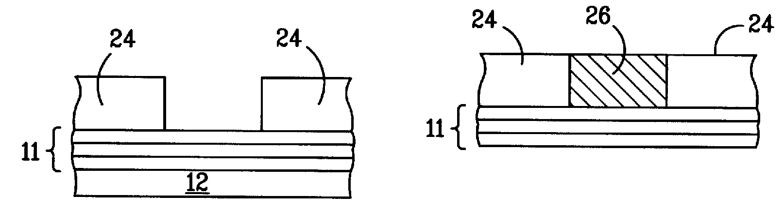
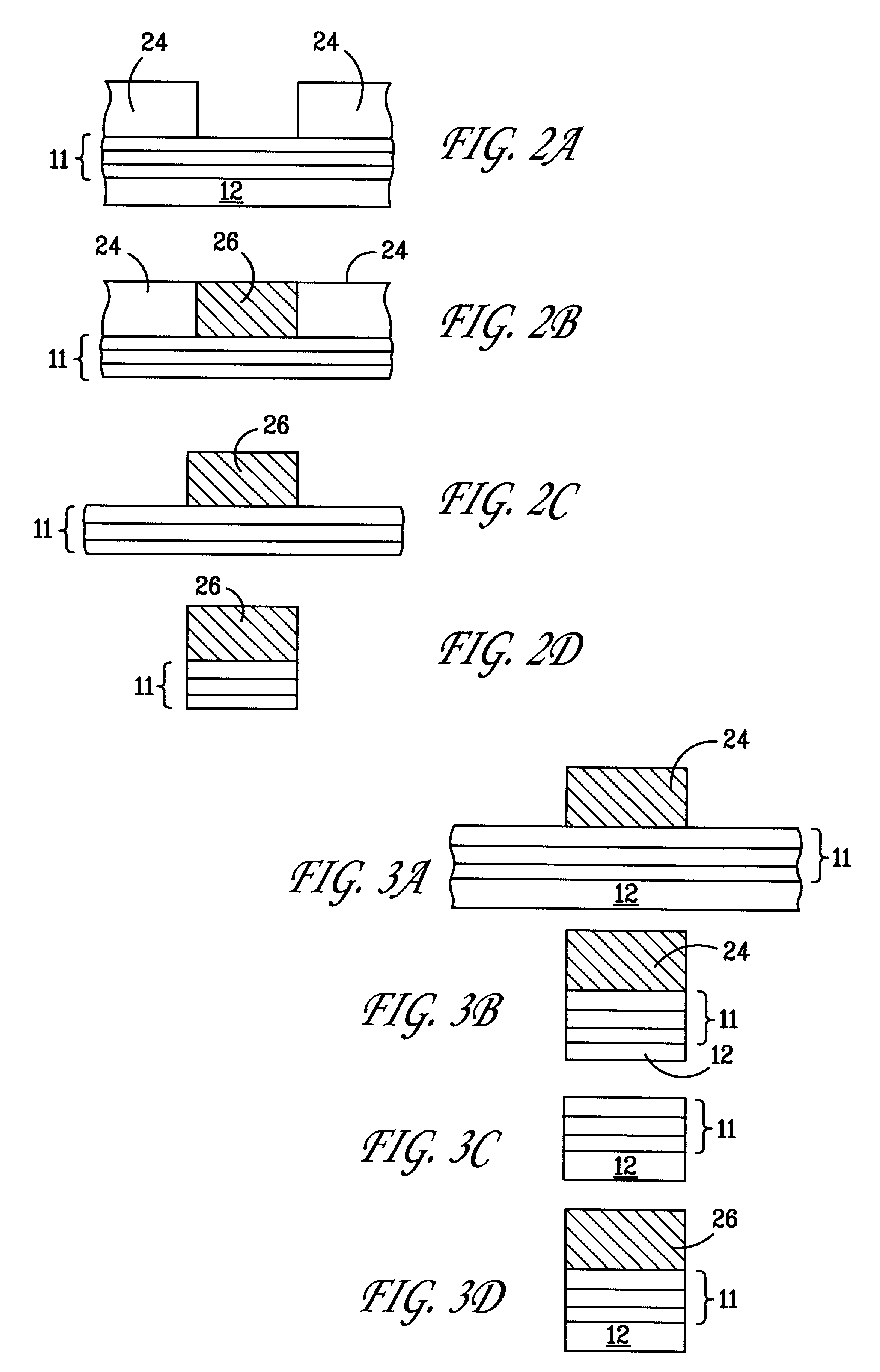
[0055]FIG. 2A to FIG. 2D illustrate steps in producing the structure of FIG. 1. In FIG. 2A the BLM 11 of FIG. ...


PUM

PropertyMeasurementUnit
thicknessaaaaaaaaaa
thicknessaaaaaaaaaa
thicknessaaaaaaaaaa

Abstract

An interconnection structure suitable for flip-chip attachment of microelectronic device chips to packages, comprising a two, three or four layer ball-limiting metallurgy including an adhesion / reaction barrier layer, and having a solder wettable layer reactive with components of a tin-containing lead free solder, so that the solderable layer can be totally consumed during soldering, but a barrier layer remains after being placed in contact with the lead free solder during soldering. One or more lead-free solder balls is selectively situated on the solder wetting layer, the lead-free solder balls comprising tin as a predominant component and one or more alloying components.

Description

FIELD OF THE INVENTION[0001]This invention relates to the interconnection of microelectronic integrated circuit (IC) devices to packages, and in particular area-array flip-chip interconnect technology often called C4 (controlled collapse chip connection). The invention further pertains to interconnection schemes that are environmentally acceptable due to the use of lead-free solder alloys and environmentally benign fabrication processes. Further, the invention pertains to interconnection schemes that eliminate sources of soft errors in on-chip circuitry through the elimination of alpha-particle sources in the solder in contact with the microelectronics circuit.BACKGROUND OF THE INVENTION[0002]In the packaging of semiconductor chips, a hierarchy of interconnections is necessary. At the level of the interconnection between the chip and the substrate (or chip carrier), three different interconnection technologies are widely employed: tape automated bonding (TAB), wire bonding, and area...

Claims


Application Information

Patent Timeline
Patent Type & Authority Applications(United States)
IPC IPC(8): H01L23/48H01L21/44
CPCH01L24/03H01L24/05H01L24/11H01L24/12H01L2224/0401H01L2224/05599H01L2224/114H01L2224/11462H01L2224/1147H01L2224/116H01L2224/13023H01L2224/13111H01L2924/01005H01L2924/01007H01L2924/01013H01L2924/01014H01L2924/01022H01L2924/01027H01L2924/01028H01L2924/01029H01L2924/01033H01L2924/0104H01L2924/01042H01L2924/01046H01L2924/01047H01L2924/0105H01L2924/01051H01L2924/01057H01L2924/01073H01L2924/01074H01L2924/01075H01L2924/01077H01L2924/01078H01L2924/01079H01L2924/01082H01L2924/01322H01L2924/01327H01L2924/014H01L2924/04953H01L2924/14H01L2924/30107H01L2924/00013H01L2924/01006H01L2924/01023H01L2924/01024H01L2924/01037H01L2924/01041H01L2924/01044H01L2924/01045H01L2924/01072H01L2224/11849H01L2224/119H01L2924/00014H01L2924/01083H01L2924/01049H01L2224/13099
Inventor BELANGER, LUCBUCHWALTER, STEPHEN L.BUCHWALTER, LEENA PAIVIKKIGIRI, AJAY P.GRIFFITH, JONATHAN H.HENDERSON, DONALD W.KANG, SUNG KWONLAINE, ERIC H.LAVOIE, CHRISTIANLAURO, PAUL A.OBERSON, VALERIE ANNESHIH, DA-YUANSRIVASTAVA, KAMALESH K.SULLIVAN, MICHAEL J.
Owner ULTRATECH INT INC
Why Eureka
Try Eureka