Semiconductor integrated circuit

a technology of integrated circuits and semiconductors, applied in the direction of power consumption reduction, pulse techniques, electric pulse generator details, etc., can solve the problems of significant increase in operation power consumption, significant decrease in operating speed, and excessively high threshold voltage of mos transistors, so as to reduce operation power consumption for signal processing and reduce fluctuation of signal delay. , the effect of high yield

Inactive Publication Date: 2008-07-24
RENESAS ELECTRONICS CORP
View PDF6 Cites 22 Cited by
  • Summary
  • Abstract
  • Description
  • Claims
  • Application Information

AI Technical Summary

Benefits of technology

[0019]That is to say, according to the present invention, it is enabled to use the substrate bias technique enabling high yield in an active mode and reduce an operation power consumption for signal processing and fluctuation of signal delay in the active mode.

Problems solved by technology

However, the dispersion in threshold voltages of the MOS transistor due to further miniaturization of semiconductor device has got obvious between chips.
That is to say, excessively low threshold voltage of the MOS transistor significantly increases operation power consumption in an active mode in which a semiconductor integrated circuit performs signal processing of a digital or an analog input signal.
On the other hand, excessively high threshold voltage of the MOS transistor significantly decreases an operating speed in an active mode in which the semiconductor integrated circuit performs signal processing of a digital or an analog input signal.

Method used


Image

  • Semiconductor integrated circuit
  • Semiconductor integrated circuit
  • Semiconductor integrated circuit

Examples


Embodiment Construction

Typical Embodiment

[0042]A typical embodiment in the inventions disclosed in the present application is briefly described. The parenthesized reference characters in the drawings to be referred in brief description of the typical embodiment merely exemplify one included in the concept of components parenthesized.

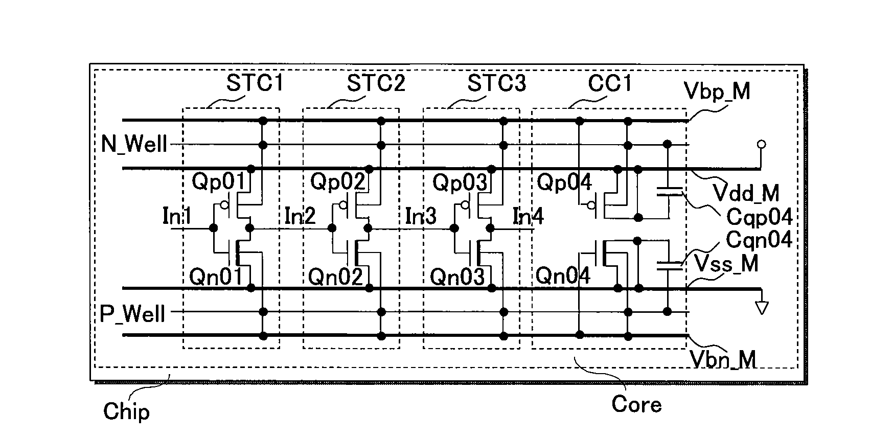
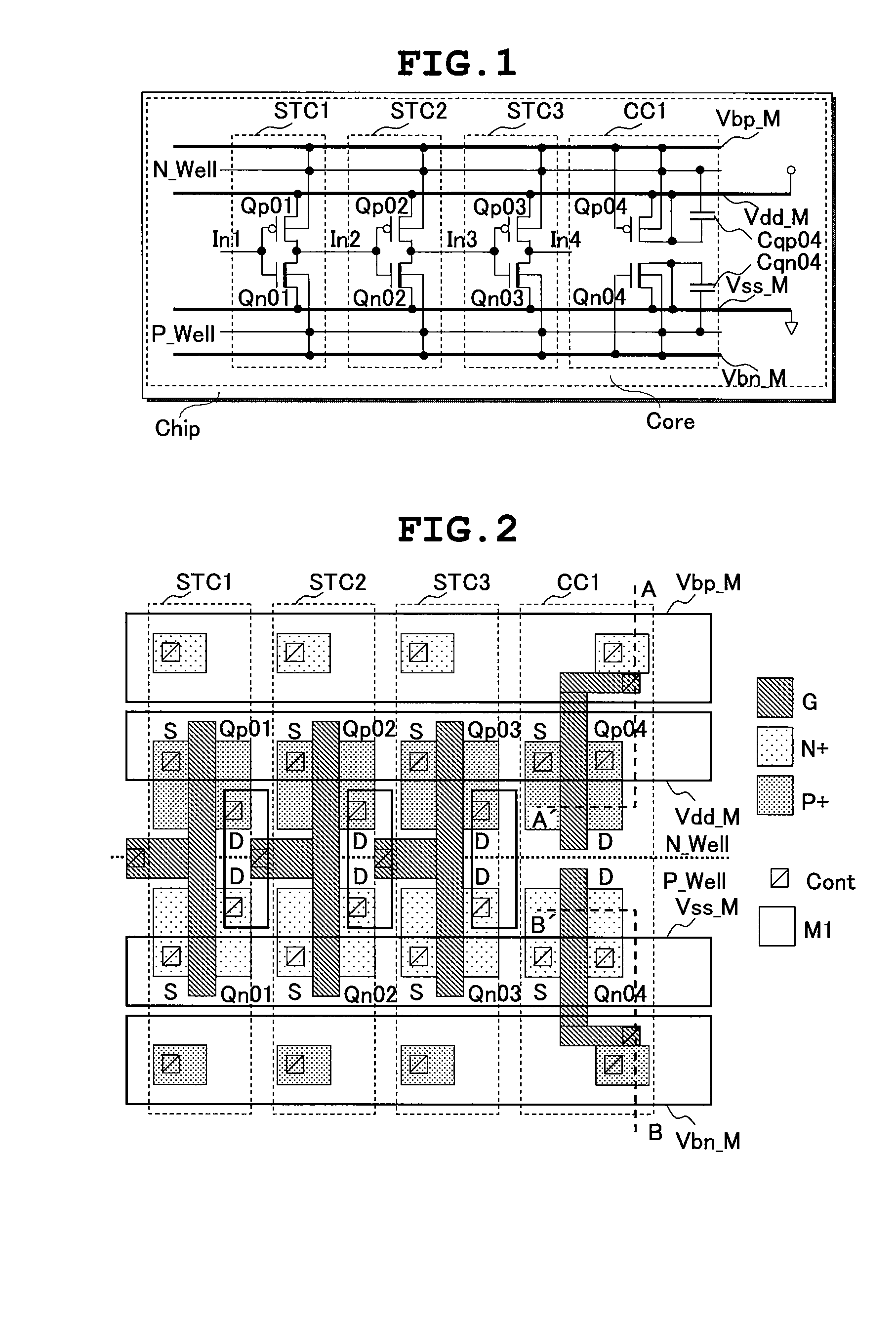
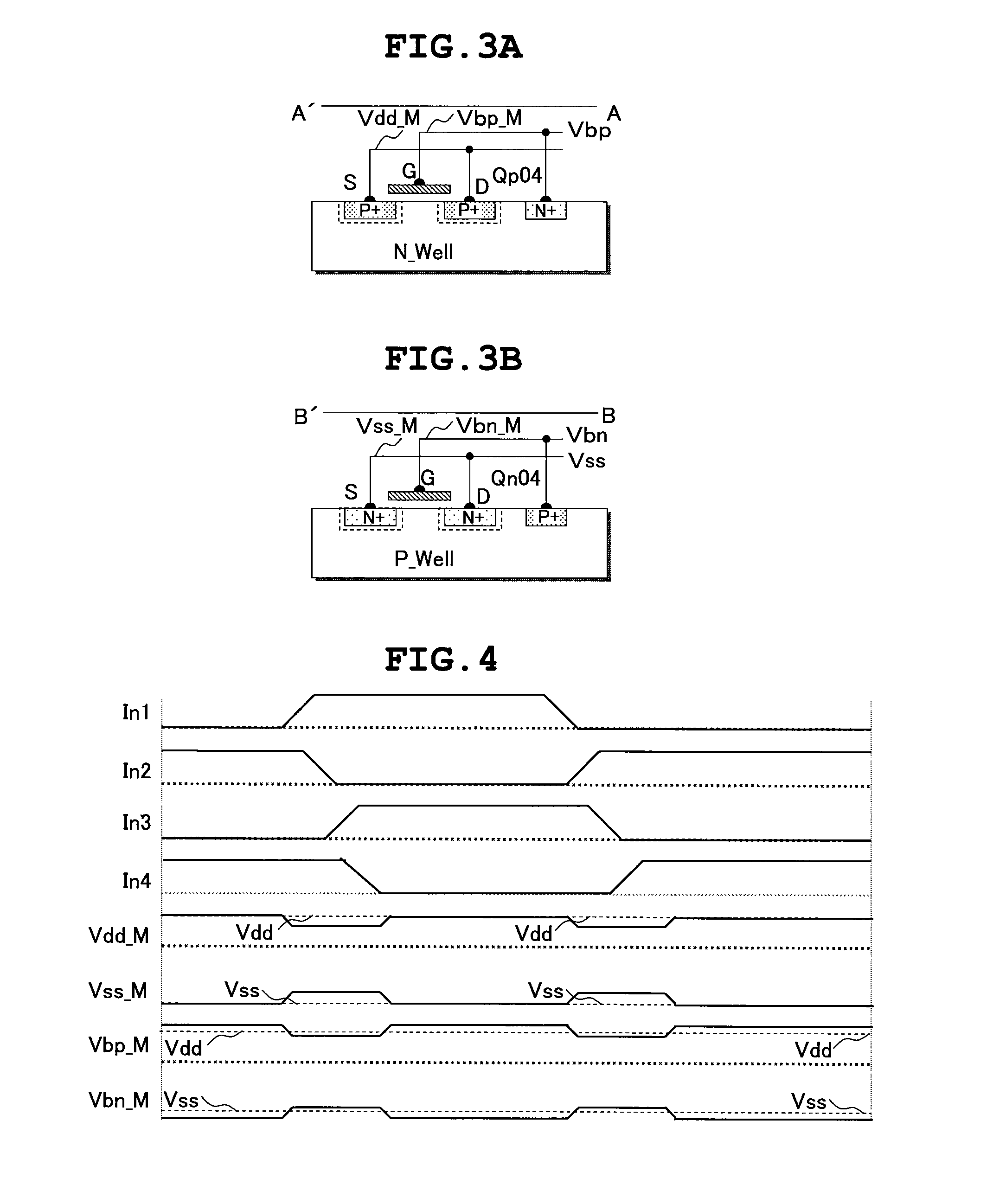
[0043][1] A semiconductor integrated circuit (Chip) according to the typical embodiment of the present invention includes a CMOS circuit (ST1, ST2 and ST3) for processing an input signal (In1) and an additional capacitance circuit (CC1) produced in the same production process as the CMOS circuit. The CMOS circuit and the additional capacitance circuit include a PMOS (Qp01, Qp02 and Qp03) and additional PMOS (Qp04) with an N well (N_Well) and a NMOS (Qn01, Qn02 and Qn03) and additional NMOS (Qn04) with an P well (P_Well). The source of the PMOS of the CMOS circuit and the source of the additional PMOS of the additional capacitance circuit are electrically coupled to a first ope...


PUM


Abstract

A substrate bias technique is used in an active mode enabling a high yield, and an operating consumption power and the fluctuation of a signal delay in signal processing are reduced in the active mode. The additional PMOS and NMOS of the additional capacitance circuit are produced in the same production process as the PMOSs and the NMOSs of the CMOS circuits. The gate capacitance of the additional PMOS is coupled between the power supply wiring and the N well and the gate capacitance of the additional NMOS is coupled between the ground wiring and the P well. The noise on the power supply wiring is transmitted to the N well through the gate capacitance and the noise on the ground wiring is transmitted to the P well through the gate capacitance. The fluctuation of noise on the substrate bias voltage between the source and the well of PMOS and NMOS of the CMOS circuits is reduced.

Description

CLAIM OF PRIORITY[0001]The present application claims priority from Japanese allocation JP 2007-013361 filed on Jan. 24, 2007, the content of which is hereby incorporated by reference into this application.FIELD OF THE INVENTION[0002]The present invention relates to a semiconductor integrated circuit, and in particular, to a technique which uses a substrate bias technique enabling high yield in an active mode and is useful to reduce an operation power consumption for signal processing and fluctuation of signal delay in the active mode.BACKGROUND OF THE INVENTION[0003]A short channel effect resulting from the miniaturization of a semiconductor device has lowered the threshold voltage of a MOS transistor and obviously increased a sub-threshold leak current. A sub threshold characteristic refers to a characteristic at not greater than the threshold voltage of the MOS transistor, and leak current generated in a weak inversion condition of a MOS silicon surface is called sub-threshold le...

Claims


Application Information

Patent Timeline
Patent Type & Authority Applications(United States)
IPC IPC(8): H03K3/01
CPCH03K2217/0018H03K19/0008H01L21/8238
Inventor OSADA, KENICHIYAMAOKA, MASANAOKOMATSU, SHIGENOBU
Owner RENESAS ELECTRONICS CORP
Why Eureka
Try Eureka