This helps you quickly interpret patents by identifying the three key elements:
Problems solved by technology
Method used
Benefits of technology
Benefits of technology
[0019]Further, in order to achieve the above object, an electronic circuit component comprises an insulator substrate, a plurality of electrodes provided on the insulator substrate, one or more elements selected from a capacitor element of dielectric material sandwiched between the electrodes, an inductor element and resistor element, a metal wiring connecting the elements, a metal terminal part of a part of the metal wiring and being arranged in a grid shape and an organic insulator material covering the elements and the circumference of the metal wiring portion excluding the metal terminal portion, with the above provision an electronic circuit component, which shows a desirable manufacturing yield and permits to integrate in a high density a variety of electronic parts such as the capacitor, inductor and resistor can be obtained and to ease connection with other parts such as a connection substrate.
[0056]Further, by arranging the respective elements separately, while sandwiching the glass substrate there between, the production process is simplified and a low cost electronic circuit component can be obtained. Further, since large distances between the respective elements can be ensured, an increase of parasitic capacity due to the coupling can be prevented.
Problems solved by technology
However the warp and size variation of the wiring materials such as the resin and the ceramics are large in comparison with those of silicon substrate which is used in the manufacture of the semiconductor integrated circuits and the formation of microscopic wirings and through holes of the order of μm by using a photolithography is impossible, therefore, it was difficult to mount the electronic parts in high density.
On the other hand, as the wiring substrate for mounting electronics parts, the general use property of the silicon substrate, which is suitable for forming the microscopic wirings is low in comparison with such as the glass epoxy substrate, and it's usage is limited.
On the other hand, the poly crystal silicon substrate can prevent in some extent the efficiency reduction, however, the poly crystal silicon substrate is more expensive than the single crystal silicon and the general use property thereof as the wiring substrate for mounting electronic parts is low and the usage thereof is limited.
However, since the heat conductivity of the ordinal glass substrate as disclosed on JP-A-2000-124358 is low and is likely broken, such as cracks and damages are frequently caused due to difference of the thermal expansion coefficients between the glass substrate and other materials (Si), as a result, yield thereof reduces and the reliability thereof also reduces.
In order to lead out the external connection terminals from the back face of the substrate, it is necessary to form through holes in the glass substrate in high accuracy, however, if a special photosensitive glass as, for example, disclosed in JP-A-9-321184 is used, the manufacturing cost of the substrate increases and it's usage is limited as the substrate for mounting the electronic parts.
Accordingly, these already known electronic circuit components do not necessarily show a high reliability, in addition, it was not necessarily easy to obtain a high manufacturing yield.
Method used
Image
Click on the blue label to locate the original text in one second.
Reading with bidirectional positioning of images and text.
Examples
embodiment 1
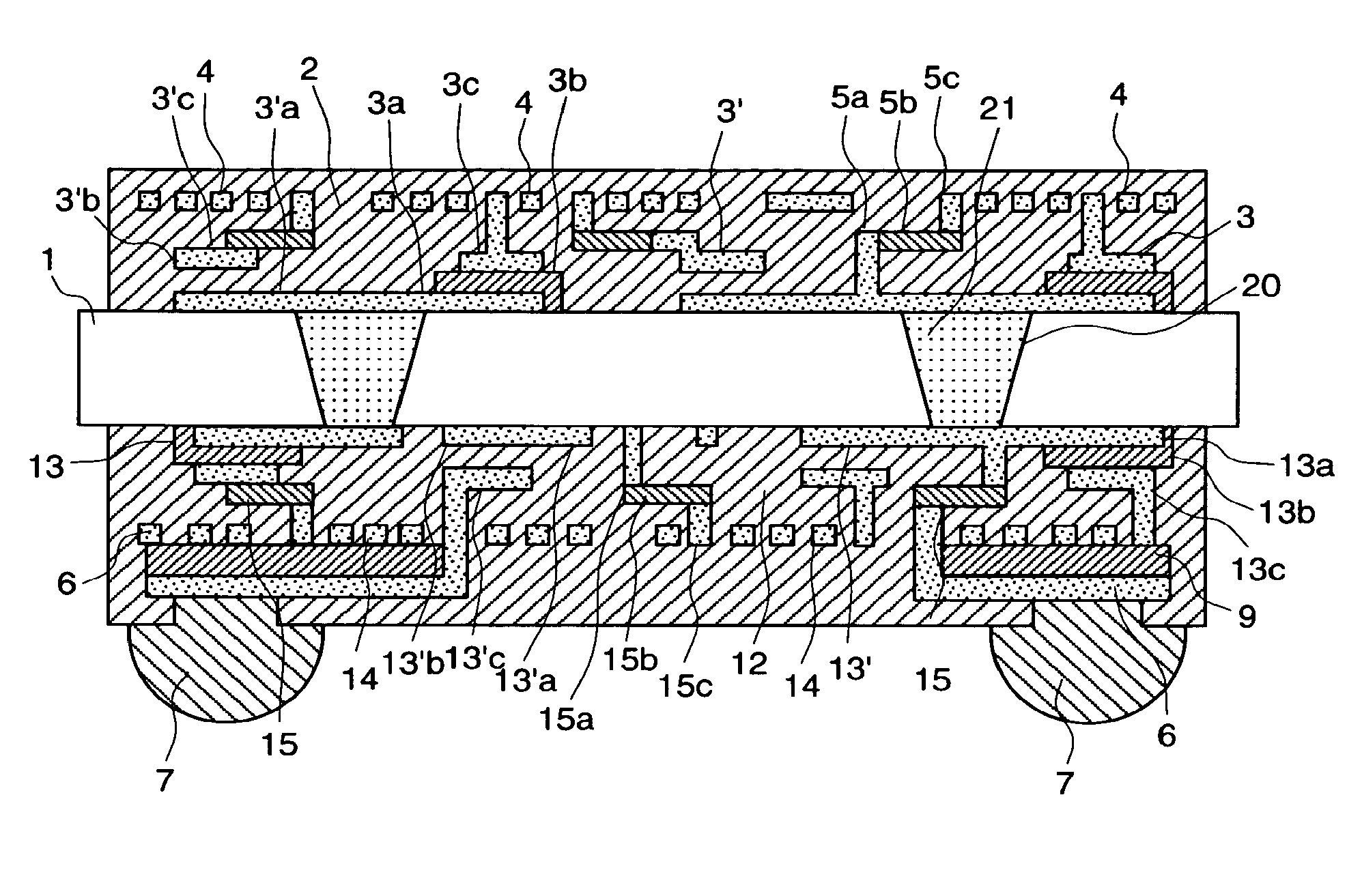
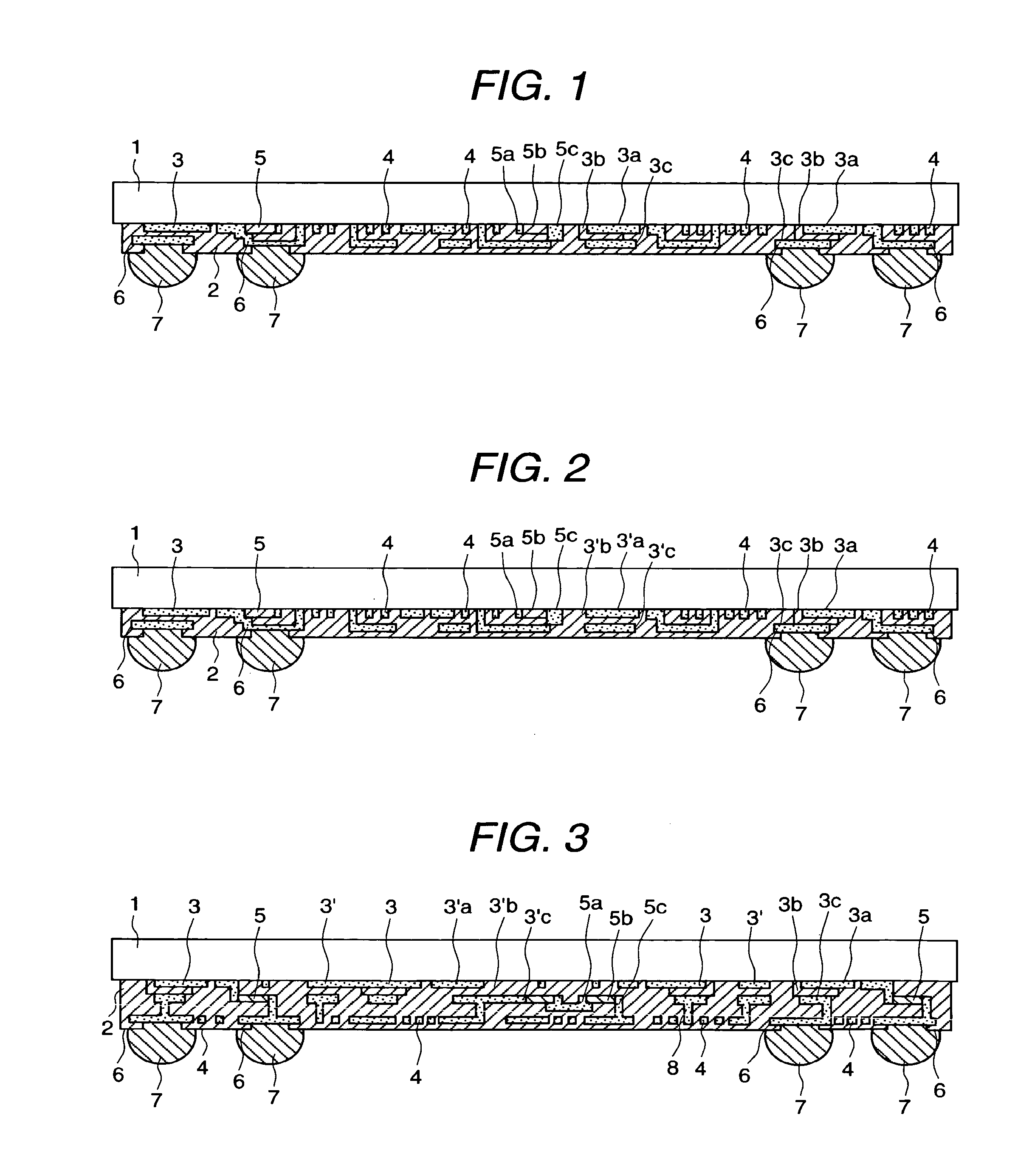
[0075]FIG. 1 is a cross sectional view of an electronic circuit component representing one embodiment of the present invention. In FIG. 1, 1 is a glass substrate (product of Nippon Electric Glass Co., Ltd., BLC), and the thickness of which is 0.5 mm.
[0076]In FIG. 1, 2 is an organic insulator and photosensitive polyimide (product of Hitachi Chemical Co., Ltd., HD-6000) is used therefor.
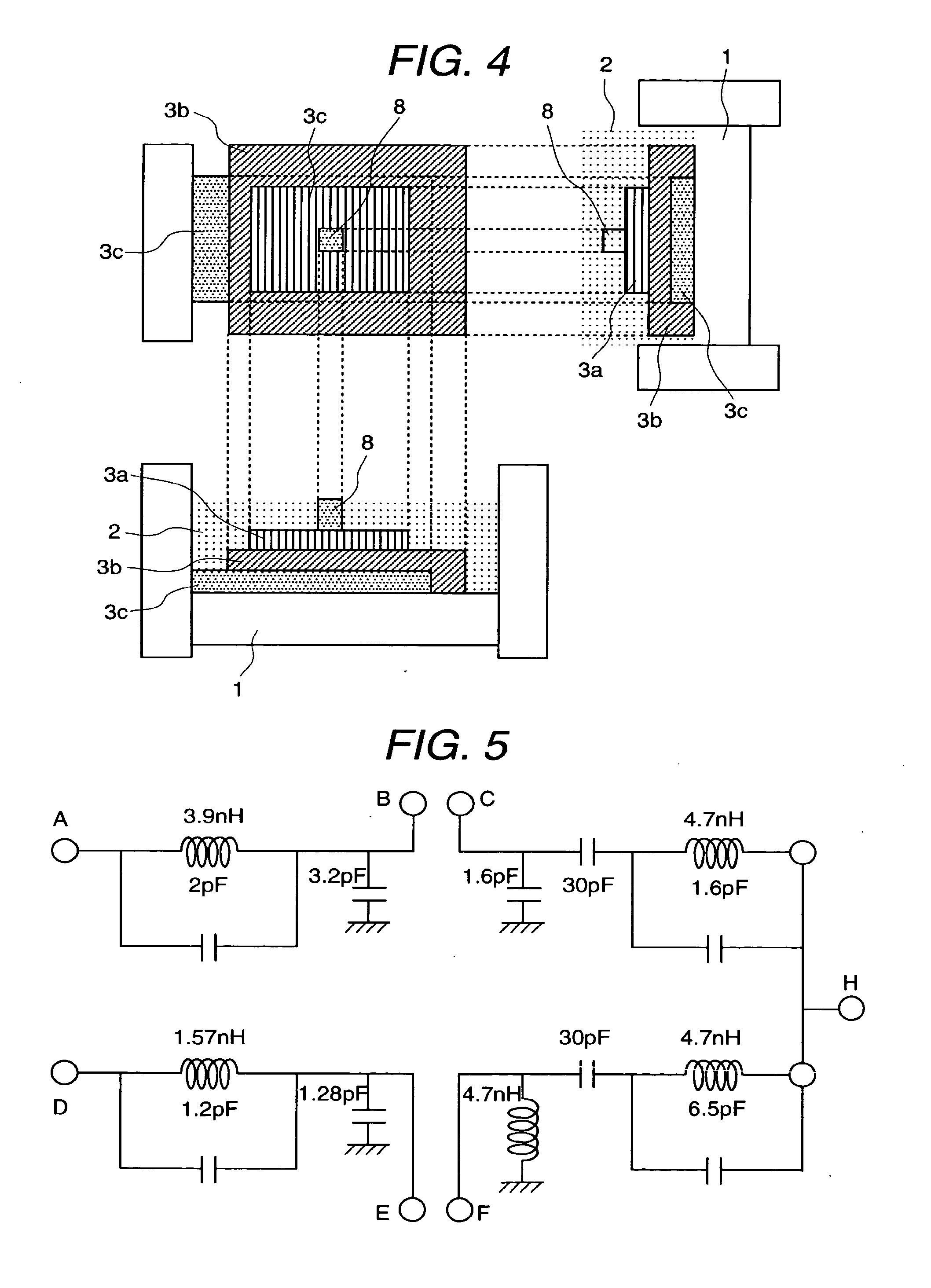
[0077]A capacitor element 3 formed inside the organic insulator 2 is in a three layer structure constituted by a lower electrode 3a, a dielectric body 3b and an upper electrode 3c. The lower electrode 3a is composed by Cu, the dielectric body 3b by oxide of Ta and the upper electrode 3c by Cu.
[0078]An inductor element 4 is a spiral type inductor and is formed on the same plane as the upper electrode 3c of the capacitor element 3 and the material thereof is Cu.
[0079]A resistor 5 is constituted by a resistance body 5b and electrodes 5a and 5c. The resistance body 5b is a compound of Ta and Ti and the ele...
embodiment 2
[0096]In embodiment 2, in place of the glass substrate 1 used in embodiment 1 in FIG. 1, the following glass substrate was used. The composition of the glass substrate of the present embodiment contains at least one rare earth element selected among the group including Sc, Y, La, Pr, Nd, Pm, Sm, Eu, Gd, Tb, Dy, Ho, Er, Tm, Yb and Lu in an amount of 0.5-20 weight % with respect to the entire glass components when converted based on oxide of Ln2O3 (Ln is a rare earth element) and as the other components contains SiO2: 40˜80 weight %, B2O3: 0˜20 weight %, R2O (R2 is alkali metal): 020 weight %, RO (R is alkaline earth metal): 0˜20 weight % and Al2O3: 0˜17 weight %, and it is preferable that R2O+RO are contained in an amount of 10˜30 weight %. Further, the thickness thereof was 0.5 mm like embodiment 1.
[0097]Further, the portions other than the glass substrate 1 in the present embodiment are the same as those in embodiment 1.
[0098]Further, the manufacturing method of the electronic circ...
embodiment 3
[0102]In embodiment 3, in place of the photosensitive polyimide used in embodiment 1, BCB (product of Dow Chemical, Cycloten 4026) was used as the organic insulator 2.
[0103]Further, the portions other than the organic insulator 2 in the present embodiment are the same as those in embodiment 1.
[0104]Further, the manufacturing method of the electronic circuit component of the present embodiment is the same as that of embodiment 1.
[0105]The dielectric constant and dielectric loss tangent of BCB are respectively 2.65 and 0.003, which are respectively smaller than 3.5 and 0.01 of the photosensitive polyimide.
[0106]Accordingly, by using BCB as an insulator layer which covers the circumference of the electronic parts, the conductive loss and dielectric loss are reduced, thereby, loss of signals passing through the electronic parts can be reduced.
[0107]Through the use of BCB for the organic insulator in the present embodiment, the conductive loss and dielectric loss are reduced, thereby, an...
PUM
Abstract
Through an improvement of module size increase due to mounting a single passive element on a substrate and an increase in the mounting cost, to provide a highly reliable, high performance and small sized electronic circuit component which permits to integrate a variety of electronic parts such as capacitors, inductors and resistors in a high density with low cost.The electronic circuit component comprises an insulator substrate, a plurality of electrodes having different areas provided on the insulator substrate, one or more elements selected from a capacitor element of dielectric material sandwiched between the electrodes, an inductor element and resistor element, a metal wiring connecting the elements, a metal terminal part of a part of the metal wiring and an organic insulator material covering the elements and the circumference of the metal wiring portion excluding the metal terminal portion.
Description
FIELD OF THE INVENTION[0001]The present invention relates to an electronic part and the manufacturing method thereof, in particular, relates to a technology which is effective when being applied to an electronic part using glass for the substrate and a manufacturing method therefore.BACKGROUND ART[0002]JP-A-8-255981 discloses a technology in which, by using an exposing process for a photo sensitive material with ultraviolet light, microscopic via holes and wirings are formed on a glass substrate. In the document, through forming a light shielding film of a metal constituting of such as Ti, Cr, Al, Ni, W, Mo, Ta and Cu on the glass substrate, multiple reflection of ultraviolet between the upper and lower faces of the glass substrate is prevented at the time of the exposing process of the photo sensitive material. Further, through forming the film thickness of the light shielding film constituted by one of the above metals more than 3 μm, the heat conductivity of the glass substrate i...
Claims
Application Information
Patent Timeline
Application Date:The date an application was filed.
Publication Date:The date a patent or application was officially published.
First Publication Date:The earliest publication date of a patent with the same application number.
Issue Date:Publication date of the patent grant document.
PCT Entry Date:The Entry date of PCT National Phase.
Estimated Expiry Date:The statutory expiry date of a patent right according to the Patent Law, and it is the longest term of protection that the patent right can achieve without the termination of the patent right due to other reasons(Term extension factor has been taken into account ).
Invalid Date:Actual expiry date is based on effective date or publication date of legal transaction data of invalid patent.

