

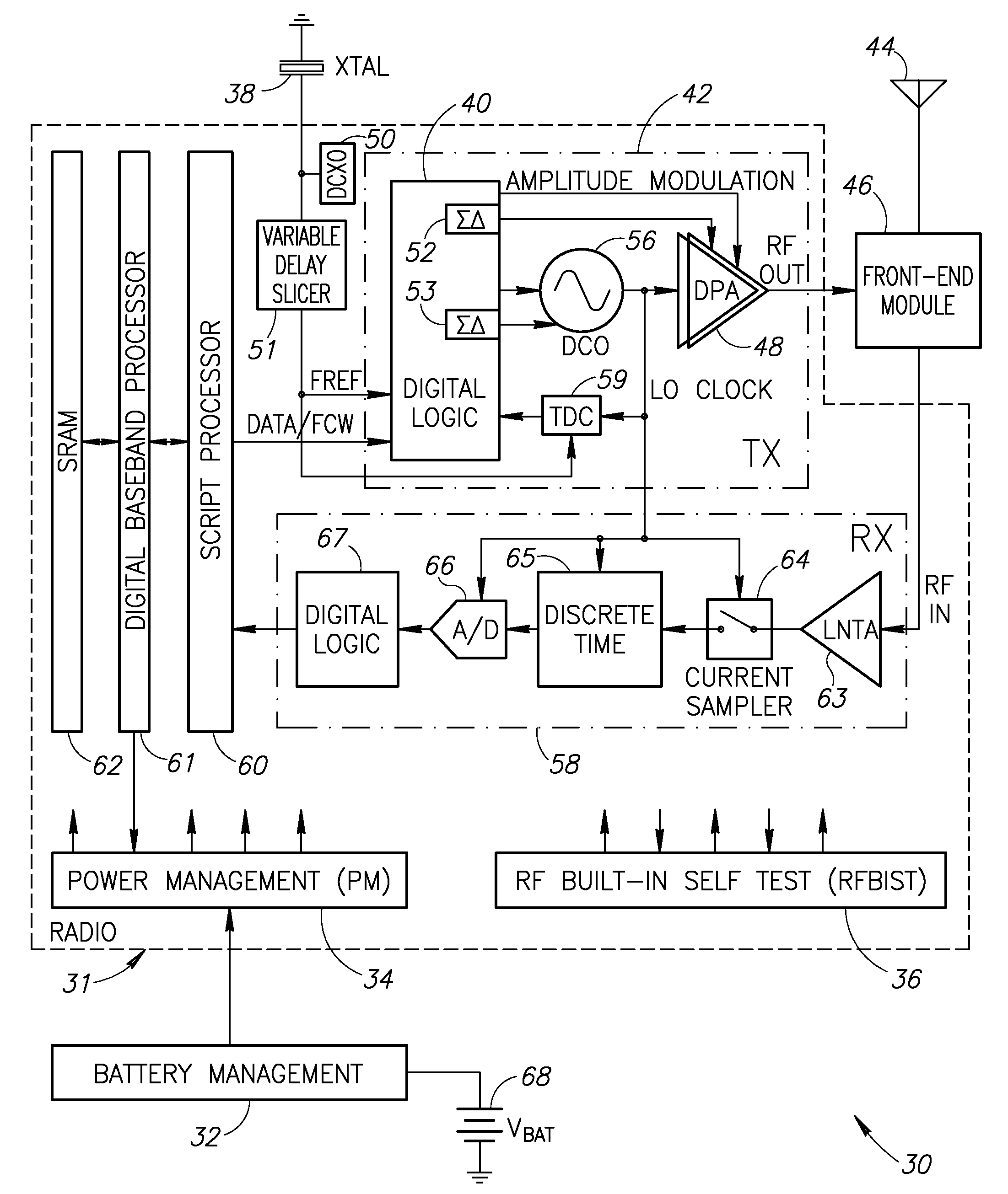
Variable delay oscillator buffer
a delay buffer and oscillator technology, applied in the field of data communication, can solve the problems of increasing the required die area, increasing the interference between the various radios (which run at different frequencies), and increasing the difficulty of system on-chip (soc) design, so as to reduce the subharmonic mixing based deterioration
- Summary
- Abstract
- Description
- Claims
- Application Information
AI Technical Summary
Benefits of technology
Problems solved by technology
Method used
Image

Examples
first embodiment
FREF Phase Dithering in a Variable Delay DCXO Buffer: First Embodiment
[0240]The spectrum R(f) of the hypothetical sampling signal r(t) in Equation 7 has been shown to be a series of Dirac functions centered at harmonics of the FREF frequency. This representation holds valid as long as the FREF signal carries no modulation, as is typically the case for a reference signal of a PLL. Once the FREF signal is purposefully frequency modulated with a phase-dithering signal, however, the sidebands of the resultant frequency modulation on the higher harmonic of it would be stronger by a factor of M (i.e. the ratio between the frequency of harmonic at M×FREF or 2×CKV, and the fundamental 26 MHz). Equivalently, the frequency deviation experienced by the Mth harmonic of FREF is M times wider. For example, consider the integer channel 1872 MHz, where N=72 and M=144, a frequency deviation of 100 Hz on FREF translates to 14.4 kHz of deviation at a second harmonic of 1872 MHz. This ‘amplified’ devia...
second embodiment
FREF Phase Dithering in a Variable Delay DCXO Buffer: Second Embodiment
[0251]A schematic diagram illustrating a second embodiment of the variable delay slicer mechanism of the present invention is shown in FIG. 15. The variable delay slicer, generally referenced 320, comprises a differential pair with PMOS input devices and is biased through a PMOS current mirror with its reference current generated through on-chip resistors. The current mirror comprises transistor MBP1 322 in series with resistor RREF 340 for generating the reference current and transistor MBP2 328 for mirroring it. The current mirror also comprises additional transistors 324, labeled MFD1 through MFDN, each in series with a respective switch 326. The differential input pair comprises transistor MP1 330 whose gate is connected to one end of the differential frequency reference output from the DCXO VOSC−, and transistor MP2 332 whose gate is connected to the other end of the differential frequency reference output f...
third embodiment
FREF Phase Dithering in a Variable Delay DCXO Buffer: Third Embodiment
[0262]In a third variable delay slicer embodiment, the first and second embodiments described supra are combined into a single circuit. A schematic diagram illustrating a third embodiment of the variable delay slicer mechanism of the present invention that combines the coarse and fine dithering into a single circuit is shown in FIG. 18.
[0263]In this combined embodiment, the variable delay slicer circuit, generally referenced 370, comprises the differential pair with controllable offset of FIG. 10 and the current mirror circuit of FIG. 15. Separate switch control circuits generate the switch sequence for the switches in the current mirror and in the differential pair portions of the circuit. In particular, coarse dither switch control circuit 382 functions to provide the coarse dither control via coarse control bits CCB(1) and CCB(2) coupled to the two switches 380. Each switch 380 controls one of the transistors 3...
PUM
 Abstract
Description
Claims
Application Information