Multidimensional Process Corner Derivation Using Surrogate Based Simultaneous Yield Analysis

a yield analysis and multi-dimensional technology, applied in process control, machine control, instruments, etc., can solve the problems of achieving reasonable yield in light of manufacturing variability, affecting the yield of semiconductor designs, and other problems, to achieve the effect of higher yield

Active Publication Date: 2008-08-14
ORACLE INT CORP
View PDF10 Cites 45 Cited by
  • Summary
  • Abstract
  • Description
  • Claims
  • Application Information

AI Technical Summary

Benefits of technology

[0015]The surrogate simulator may in some embodiments be used to simulate a manufacturing process shift by modifying the distribution in the simulation to shift or exaggerate the range of inputs, or to focus on a particular region of interest, for example. Using this approach a designer may be able to reasonably assess yield under process drift and determine how the process may be shifted to achieve higher yield.

Problems solved by technology

In deep submicron processes, the issue of achieving reasonable yield in light of manufacturing variability is a considerable challenge.
In such technologies, channel dopants are in concentrations on the order of fewer than 100 atoms with uncontrollable fluctuations from one device to another; line-width Cd-Variation becomes nearly impossible to control despite recent advances in lithography techniques; leakage is unlike anything seen before; and electrons exhibit direct tunneling through dielectrics as if they were not even there, for example.
In addition to these limitations of solid state device physics, manufacturing technologists face other difficulties in fabricating circuit structures, as evidenced by fabrication topics of late: Ultra-deep ultra-violet lithography, Optical Phase Correction (OPC), Stepper Control, Phase Shift Masks (PSM), Chemical Mechanical Polishing (CMP), Depth of Field correction (DOF), immersion lithography, etc.
These issues add up to uncertainty, variation, and great difficulty in controlling and managing the manufacturing process, which can result in tremendous yield loss.
This is a reasonable approach but is greatly limited to smaller circuits that may not represent the semiconductor device (e.g., a microprocessor) as a whole.
These general-purpose corners are often non-physical and / or unrealistic, and may not explore the sensitivities that are critical to the metrics of concern for a given circuit or circuit path.
If not, achieving a reasonable yield becomes a trade-off exercise, which could be so severe as to produce a non-overlapping zero-yielding solution.
Using prior art methods, simulations were only done in isolation and could only assess yield for individual circuit metrics.
Therefore, prior art solutions often fail to identify sensitivities and critical aspects as they pertain to a particular individual circuit and to an entire semiconductor device as a whole.
The method includes deriving highly significant corners by simulating the device using a surrogate model, rather than by performing a full Monte Carlo analysis, since a full Monte Carlo analysis may not be feasible for simulation and verification of large circuits and circuit paths.
For example, some combinations of device parameter values are not physically possible (or not physically likely), while other combinations work together to improve or hinder performance.

Method used


Image

  • Multidimensional Process Corner Derivation Using Surrogate Based Simultaneous Yield Analysis
  • Multidimensional Process Corner Derivation Using Surrogate Based Simultaneous Yield Analysis
  • Multidimensional Process Corner Derivation Using Surrogate Based Simultaneous Yield Analysis

Examples


Embodiment Construction

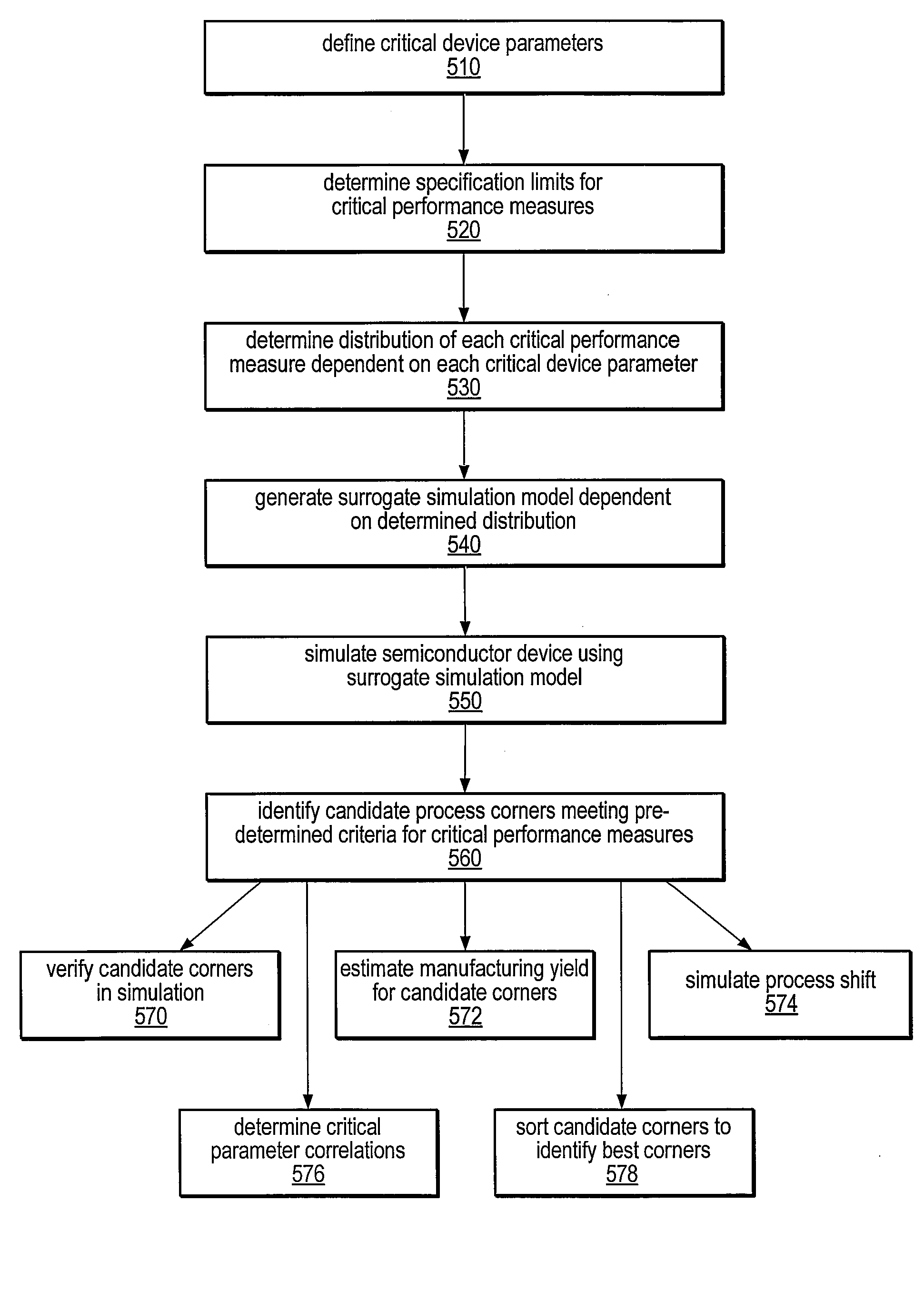
[0030]During the design of semiconductor devices, circuit simulations (e.g., post-layout circuit simulations) may be performed using a net-list extracted from the design layout, and may provide an assessment of the circuit speed, the influence of circuit parasitics (such as parasitic capacitances and resistances), and any glitches that may occur due to signal delay mismatches. Any circuit sensitivities identified by during simulation may be corrected using an iterative approach until the simulations indicate that the device is likely to meet functionality and performance goals and to yield reasonably well. Once these simulations are complete (and any identified design rule errors are corrected), the design may be ready for fabrication and may be sent to a fabrication facility.

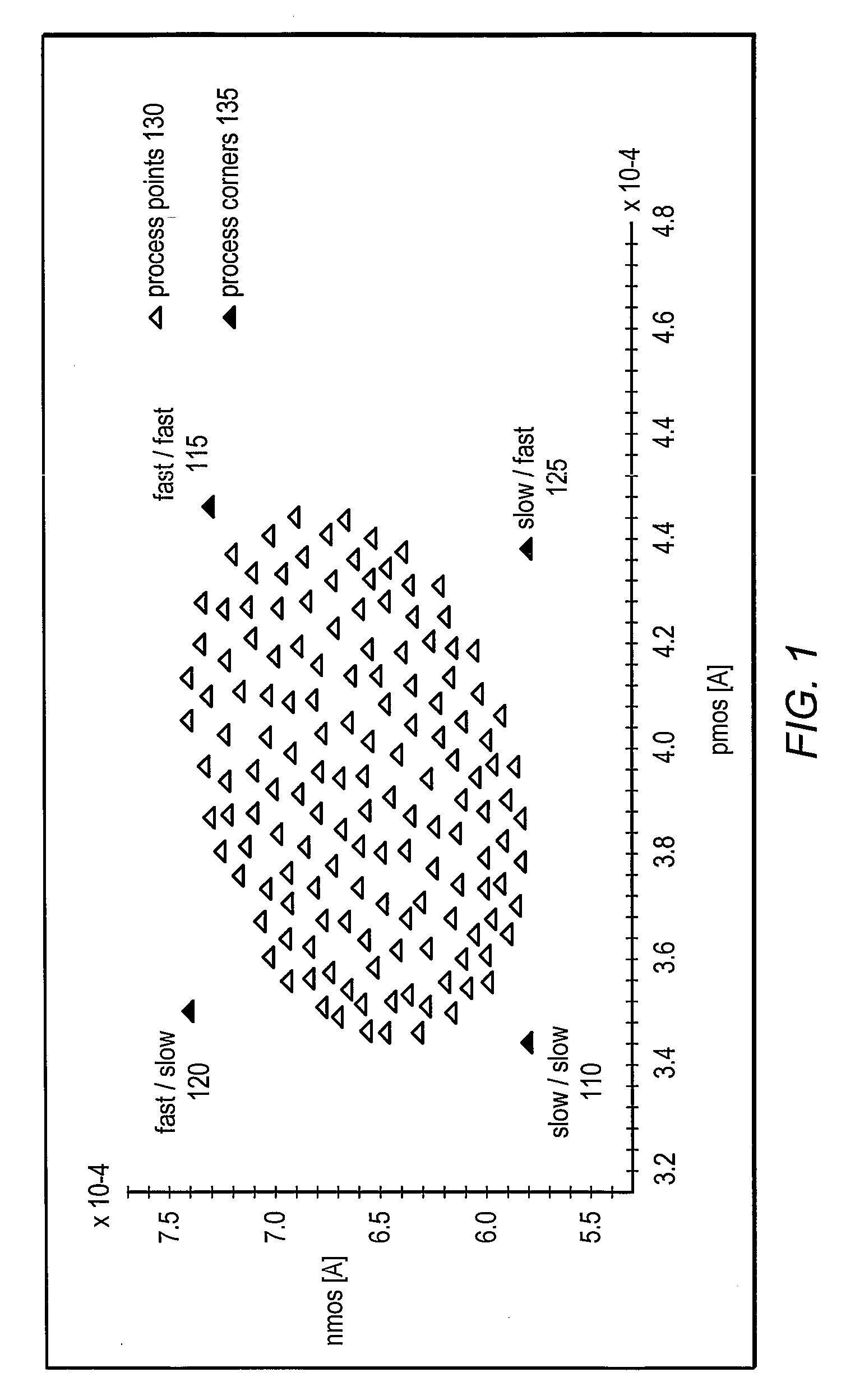
[0031]Traditionally, process corners (e.g., typical, best-case, and worst-case process parameter combinations) have been chosen for circuit simulations based on simulations and / or yield data related to individu...


PUM


Abstract

A system and method for deriving semiconductor manufacturing process corners using surrogate simulations is disclosed. The method may be used to determine individual performance metric yields, the number of out-of-specification conditions for a given number of simulation samples, and a total yield prediction for simultaneous multi-variable conditions. A surrogate simulation model, such as a Response Surface Model, may be generated from circuit simulation data or parametric data measurements and may be executed using a large number of multi-variable sample points to determine process corners defining yield limits for a device. The model may also be used to simulate process shifts and exaggerated input ranges for critical device parameters. In some embodiments, the derived process corners may better represent physically possible worst-case process corners than traditional general-purpose process corners, and may address differences in process sensitivities for individual circuits of the device.

Description

BACKGROUND OF THE INVENTION[0001]1. Field of the Invention[0002]This invention relates to semiconductor design and more specifically to yield analysis for manufacturing of semiconductor designs.[0003]2. Description of the Relevant Art[0004]In deep submicron processes, the issue of achieving reasonable yield in light of manufacturing variability is a considerable challenge. At approximately the 130 nm process node, the underlying physics and quantum mechanical effects begin to govern the behavior of CMOS technology and the ability to dictate and predict the desired behavior begins to decline. In such technologies, channel dopants are in concentrations on the order of fewer than 100 atoms with uncontrollable fluctuations from one device to another; line-width Cd-Variation becomes nearly impossible to control despite recent advances in lithography techniques; leakage is unlike anything seen before; and electrons exhibit direct tunneling through dielectrics as if they were not even ther...

Claims


Application Information

Patent Timeline
Patent Type & Authority Applications(United States)
IPC IPC(8): G06F17/10G06G7/48G06F17/50
CPCG05B17/02G05B15/02
Inventor BARKER, AARON J.RUSSELL, EDMUND L.
Owner ORACLE INT CORP
Why Eureka
Try Eureka