Phototransistors, Methods of Making Phototransistors, and Methods of Detecting Light

Inactive Publication Date: 2008-08-28
ADVANCED OPTICAL MATERIALS
View PDF4 Cites 21 Cited by
  • Summary
  • Abstract
  • Description
  • Claims
  • Application Information

AI Technical Summary

Benefits of technology

[0014]The present invention provides phototransistors having sensitivity to light at wavelengths >1.8 micrometer, especially at wavelengths of 2.0 micrometers and above. The present invention further provides phototransistors having high responsivity, low noise, high internal gain and/or large dynamic range. The word “internal” in the expression “internal gain” indicates that no external amplifiers and thus external gain are involved, and that the gain is provi

Problems solved by technology

Strained InGaAs layers (not lattice matched to InP substrates) are used in these devices, which results in non-optimized device properties, such non-optimized device properties coming from non-optimal materials properties which result from lattice mismatch.
Commercially available extended wavelength InGaAs and HgCdTe detectors are described as providing 2 micrometer sensitivity, but due to the absence of an internal gain mechanism, these detectors lack sufficient responsivity.
Without providing these properties, avalanching either does not start or proceeds loca

Method used


Image

  • Phototransistors, Methods of Making Phototransistors, and Methods of Detecting Light
  • Phototransistors, Methods of Making Phototransistors, and Methods of Detecting Light
  • Phototransistors, Methods of Making Phototransistors, and Methods of Detecting Light

Examples


Example

EXAMPLE

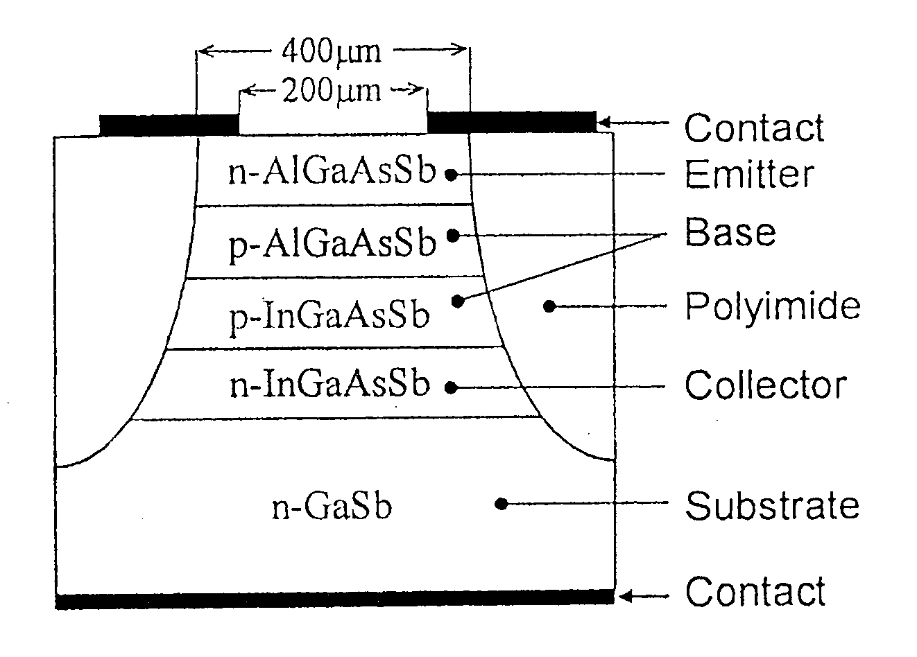
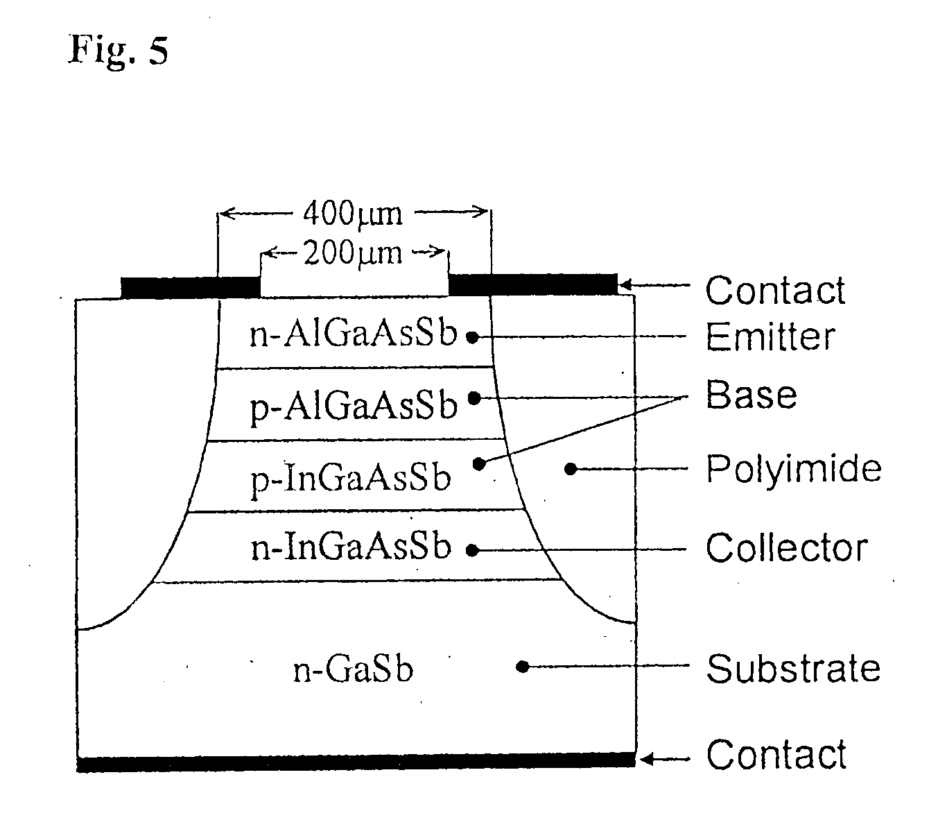
[0088]A device according to the present invention was constructed to he as depicted in FIG. 5. The device according to the present invention used in this Example includes an n-type AlGaAsSb emitter, a p-type composite base consisting of AlGaAsSb and InGaAsSb layers, and an n-type InGaAsSb collector. The collector, the base and the emitter were all lattice-matched to a GaSb substrate and were grown by liquid-phase epitaxy using a horizontal slideboat technique. The bandgap energies of the AlGaAsSb and InGaAsSb layers are 1-1.1 eV and 0.55 eV, respectively, as estimated from chemical composition and spectral response measurements. Mesa phototransistors with a 400 μm diameter total area and a 200 μm diameter active area were defined using photolithography and wet chemical etching. A backside planar and a front side annular ohmic contact, including a bonding pad, were deposited by electron beam evaporation of Au / Sn and Ti / Ni / Au, respectively. A polyimide coating (HD Microsystems ...


PUM


Abstract

A phototransistor (400) comprises an emitter (43) comprising antimony, a base (42) comprising antimony, and a collector (41) comprising antimony. Preferably, the emitter, the base and the collector each comprises at least one of AlInGaAsSb, AlGaAsSb, AlGaSb, GaSb and InGaAsSb. The base comprises an emitter-contacting portion (41b) with a base-contacting portion (43a) of the emitter. The collector comprises a base-contacting portion (41b) which is in contact with a collector-contacting portion (421a) of the base. The phototransistor produces an internal gain upon being contacted with light within a receivable wavelength range, preferably greater than 1.7 micrometers. Also, a method of detecting light using such a phototransistor.

Description

CROSS-REFERENCE TO RELATED APPLICATIONS[0001]This application claims the benefit of U.S. Provisional Patent Application Ser. No. 60 / 538,483, filed Jan. 22, 2004, the entirety of which is incorporated herein by reference.FIELD OF THE INVENTION[0002]The present invention relates to phototransistors. In particular, the present invention relates to phototransistors having sensitivity to light at wavelengths greater than 1.8 micrometers, preferably in the range of 1.8 micrometers to 2.5 micrometers.BACKGROUND OF THE INVENTION[0003]Photodetectors which are sensitive at wavelengths >1.8 micrometers, in particular >2.0 micrometers, and which exhibit internal gain, are highly desirable.[0004]InGaAs has been studied as a potential material for this application, but to reach sensitivity at wavelengths >1.7 micrometers, so-called extended wavelength InGaAs photodetectors are necessary. Strained InGaAs layers (not lattice matched to InP substrates) are used in these devices, which resul...

Claims


Application Information

Patent Timeline
IPC IPC(8): H01L31/0304H01L31/11G01J1/02H01L31/0328H01L31/06
CPCH01L31/03046Y02E10/544H01L31/1105
Inventor SULIMA, OLEG
Owner ADVANCED OPTICAL MATERIALS
Why Eureka
Try Eureka