Light emitting device

a light-emitting device and light-emitting layer technology, applied in the direction of semiconductor devices, basic electric elements, electrical equipment, etc., can solve the problems of large apparatus, large amount of time required to remove air, uneven surface of metal powder, etc., to improve the light-emitting efficiency of organic light-emitting layer, low work function of electrode layer, and low electron injection energy

Inactive Publication Date: 2008-09-04
ALPS ALPINE CO LTD
View PDF3 Cites 14 Cited by
  • Summary
  • Abstract
  • Description
  • Claims
  • Application Information

AI Technical Summary

Benefits of technology

[0010]The present invention has been finalized in view of the drawbacks inherent in the conventional light emitting device, and it is an object of the present invention to provide a light emitting device capable of forming a light-emitting layer and an electrode layer in the air. Another object of the present invention is to provide an electrode having a low work function while exposed to the air in order to improve the light emitting efficiency of a light-emitting layer.
[0023]According to the invention, since the auxiliary electrode layer is formed of a conductive metal interposed between the organic light-emitting layer and the lower electrode layer or the counter electrode layer, it is possible to make the work function of the electrode layer low, to make electron injection energy low, and to improve the light emitting efficiency of the organic light-emitting layer. Further, it is possible to form all of the lower or counter electrode layer and the auxiliary electrode layer under air pressure. Furthermore, since the auxiliary electrode layer has small asperity, it is possible to reduce the thickness of the organic light-emitting layer provided on or underneath the auxiliary electrode layer. As a result, the movement distance of electrons and holes is reduced, which makes it possible to reduce energy loss and to improve the light emitting efficiency.

Problems solved by technology

However, in order to perform, for example, the vapor deposition process in a vacuum, a large apparatus is required and a large amount of time is required to remove the air.
However, since the diameter of a particle of the metal powder is large, that is, the particle has a diameter of several microns, the surface of the metal powder is uneven.
Further, since the organic material exists between the particles of the metal powder, it is difficult to obtain a layer made of only the metal and to form a dense layer.
Since it is difficult to form a dense layer, it is difficult to prevent inflow of oxygen or moisture.
Thus, external oxygen or moisture easily reaches the light-emitting layer through the metal layer, resulting in oxidization of the light-emitting layer.
However, since the cathode layer is easily oxidized, it needs to be formed using a high vacuum by, for example, the sputtering method or the vapor deposition method, and a method of forming a cathode layer at atmospheric pressure has not yet been established.
Therefore, even though it is possible to from the organic light-emitting layer under atmospheric pressure by, for example, a printing technique, due to the electrode layers on both sides of the organic light-emitting layer being formed by, for example, the vacuum deposition method or the sputtering method, it is difficult to form the light-emitting layer and the electrode layers under atmospheric pressure all once.
Therefore, after the electrode layers are formed in a vacuum, the light-emitting layer is formed under high atmospheric pressure, or the electrode layers are formed by reducing the atmospheric pressure to vacuum pressure, which requires considerable forming time.
Further, since the material used for the cathode easily oxidizes, it is required to seal the light emitting device so as to prevent oxygen or moisture from entering therein.
However, since it is difficult to completely shield the light emitting device from oxygen and moisture by such a method, a method of adhering a substrate to a stainless can filled with an absorbent material has been used.

Method used


Image

  • Light emitting device
  • Light emitting device
  • Light emitting device

Examples


example 1

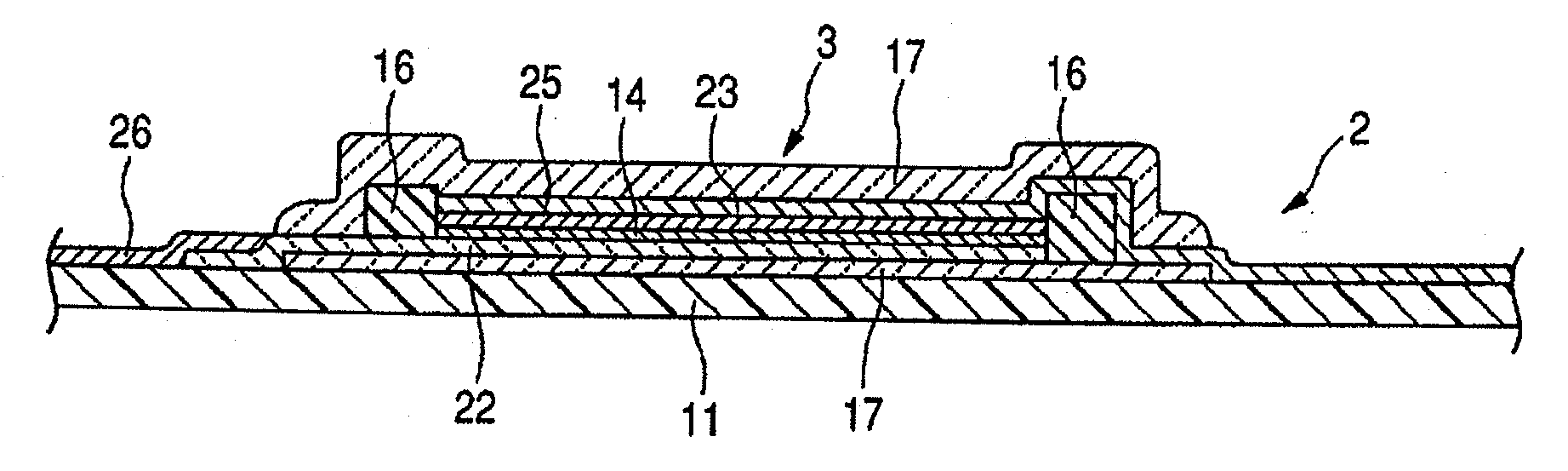
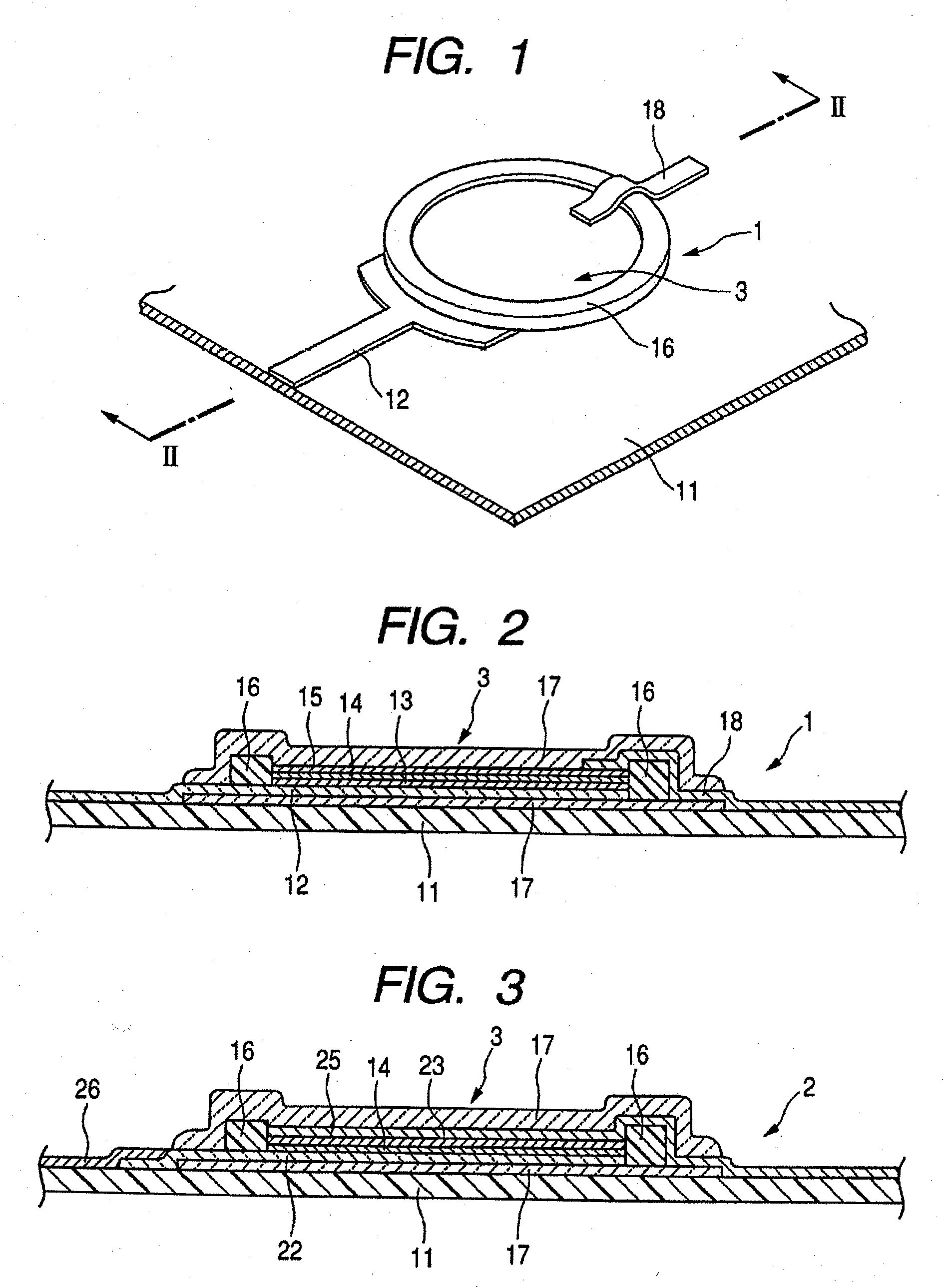
[0062]A solution of tetraethoxysilane is applied on a PET film (Lumirror U94 made by Toray industries, Inc.) to have a thickness of 100 μm by a tubing dispenser (made by Musashi engineering, Inc.), and a heating process is performed at a temperature of 120° C. for half an hour, thereby forming the sealing layer 17 of glass. The tetraethoxysilane solution contains 1% by mass of acetic acid.

[0063]As shown in FIG. 1, screen printing is performed on SW1300 (made by Asahi Chemical Research Laboratory Co., Ltd.), in which a polyester resin binder and silver particles are contained in a circular region, by using a 400-mesh stainless screen printing plate. Then, a heating process is performed under dry air at a temperature of 110° C. for half an hour. In this way, the lower electrode layer 12 is formed.

[0064]Subsequently, the bank (sealing wall) 16 for defining a circular light-emitting region 3 (having a diameter of 5 mm to 10 mm) is formed by screen printing. The bank 16 is formed of FR-1...

example 2

[0073]Using the same materials as Example 1, the bottom emission type light emitting device shown in FIG. 3 is fabricated. When a voltage of 20 V is applied to the transparent electrode layer 22 (anode), serving as a lower electrode layer, and the counter electrode layer 25 (cathode), serving as an upper electrode layer, green light with a brightness of 15 cd(candelas) / m2 is emitted. The half-life of the brightness is 4 days.

example 3

[0074]The light emitting device as shown in FIG. 2 is fabricated in the same manner as Example 1 except that Fine Sphere SVE102 made by Nippon Paint Co., Ltd. is used as the colloidal nano silver ink without adding potassium acetate thereto. When a voltage of 20 V is applied to the upper transparent electrode layer (anode) and the lower electrode layer (cathode), green light with a brightness of 20 cd(candelas) / m2 is emitted. The half-life of the brightness is 3 days.


PUM


Abstract

A light emitting device includes a laminate of a lower electrode layer, an organic light-emitting layer, and an upper transparent electrode layer. In the light emitting device, an auxiliary electrode layer is formed of colloidal nano-sized particles of a conductive metal between the lower electrode layer and the organic light-emitting layer. The auxiliary electrode layer causes the lower electrode layer to be flat and the light emitting efficient to be improved. A light emitting device having a structure in which a transparent electrode layer is formed as the lower electrode layer, and an organic light-emitting layer, an auxiliary electrode layer, and an upper electrode layer are sequentially formed thereon has the same effects. When glass is produced by a sol-gel method using metal alkoxide and the light emitting device is sealed by the glass, it is possible to extend the light emitting period.

Description

[0001]This application claims the benefit of U.S. application Ser. No. 11 / 565,417 filed on Nov. 30, 2006, which claims the benefit of Japanese Patent Application Nos. 2005-345043 and 2005-345046, filed on Nov. 30, 2005, both of which are hereby incorporated by referenceBACKGROUND OF THE INVENTION[0002]1. Field of the Invention[0003]The present invention relates to a light emitting device using an organic light-emitting layer, and more specifically, a light emitting device that includes: a lower electrode layer disposed inside a light-emitting region surrounded by a bank (sealing wall); an organic light-emitting layer provided on the lower electrode layer; and a transparent electrode layer provided on the organic light-emitting layer. Also, the present invention relates to a light emitting device that includes: a transparent electrode layer disposed inside a light-emitting region; an organic light-emitting layer provided on the transparent electrode layer; and a counter electrode lay...

Claims


Application Information

Patent Timeline
Patent Type & Authority Applications(United States)
IPC IPC(8): H01L51/56
CPCH01L51/5237H01L51/5203H10K50/805H10K50/844
Inventor ASABE, YOSHIYUKI
Owner ALPS ALPINE CO LTD
Why Eureka
Try Eureka