Manufacturing method of semiconductor device

a manufacturing method and semiconductor technology, applied in the direction of semiconductor devices, basic electric elements, electrical equipment, etc., can solve the problems of difficult to form a crystalline semiconductor film, deterioration of electrical characteristics of thin film transistors, and increased trap level at grain boundaries, so as to reduce the viscosity of semiconductor melt and suppress the turbulence of semiconductor mel

Inactive Publication Date: 2008-09-04
SEMICON ENERGY LAB CO LTD
View PDF99 Cites 25 Cited by
  • Summary
  • Abstract
  • Description
  • Claims
  • Application Information

AI Technical Summary

Benefits of technology

[0019]That is, the amount of energy of a laser beam which is absorbed by the semiconductor film is controlled with a scanning rate and power of the laser beam with the cap film formed over the semiconductor film, whereby reduction in viscosity of the melt of the semiconductor can be suppressed, turbulence of the melt of the semiconductor can be suppressed, and orientations of crystal planes and the size of a crystal grain of a crystalline semiconductor film can be controlled. As a result, a crystalline semiconductor film which has large grain crystals and in which orientations of crystal planes are controlled can be formed.
[0020]In addition, the cap film is formed over the semiconductor film and the semiconductor film is irradiated with a continuous-wave laser beam or a pulsed laser beam with a repetition rate of greater than or equal to 10 MHz of which power and scanning rate are controlled, whereby controls of generation of crystal nuclei, viscosity of the melt of the semiconductor, the amount of energy which is absorbed by the semiconductor film, the amount of melting time of the semiconductor film, and the like become possible. As a result, orientations of crystal planes and the grain size of the crystal can be controlled.

Problems solved by technology

In addition, when there is a plurality of crystals having different orientations of crystal planes in the channel formation region of the thin film transistor, a trap level at grain boundaries is increased; thus, electrical characteristics of the thin film transistor are deteriorated.
Moreover, it is difficult to form a crystalline semiconductor film provided with crystals having an orientation of crystal planes which is suitable for an n-type thin film transistor and crystals having an orientation of crystal planes which is suitable for a p-type thin film transistor.

Method used


Image

  • Manufacturing method of semiconductor device
  • Manufacturing method of semiconductor device
  • Manufacturing method of semiconductor device

Examples


embodiment mode 1

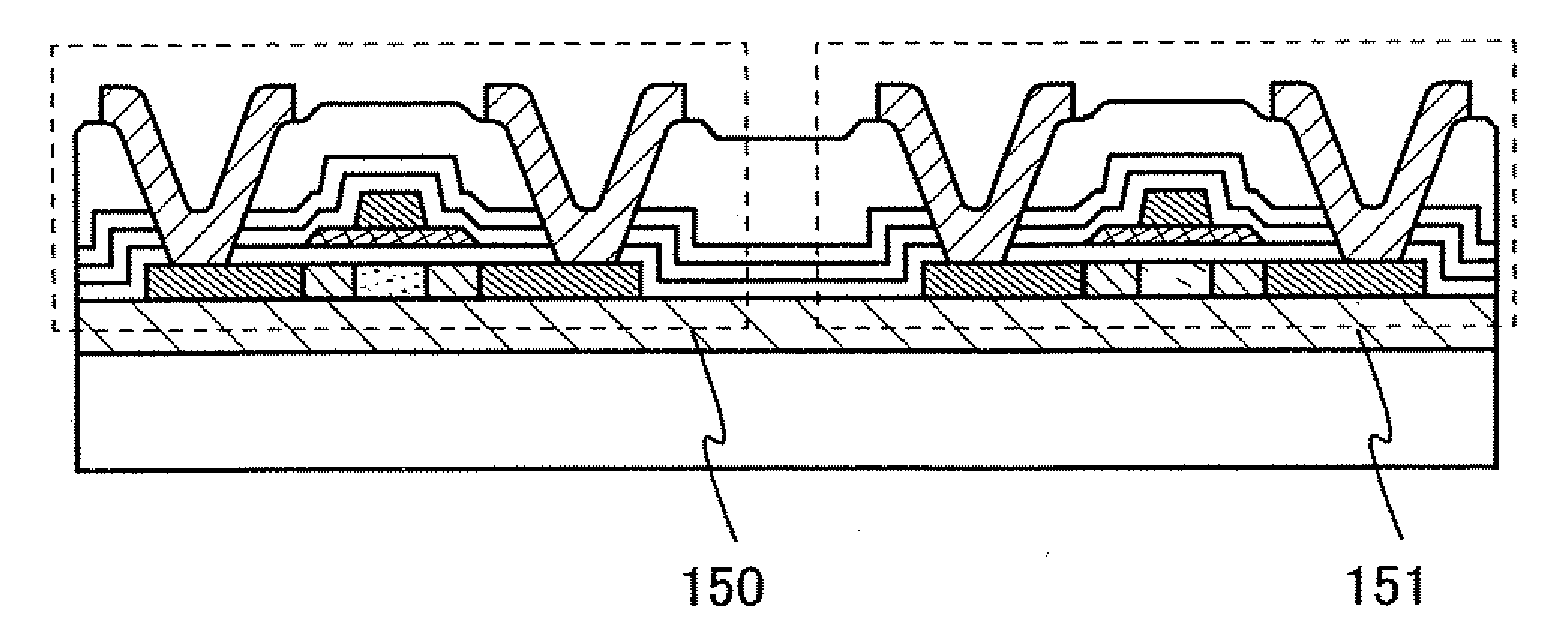
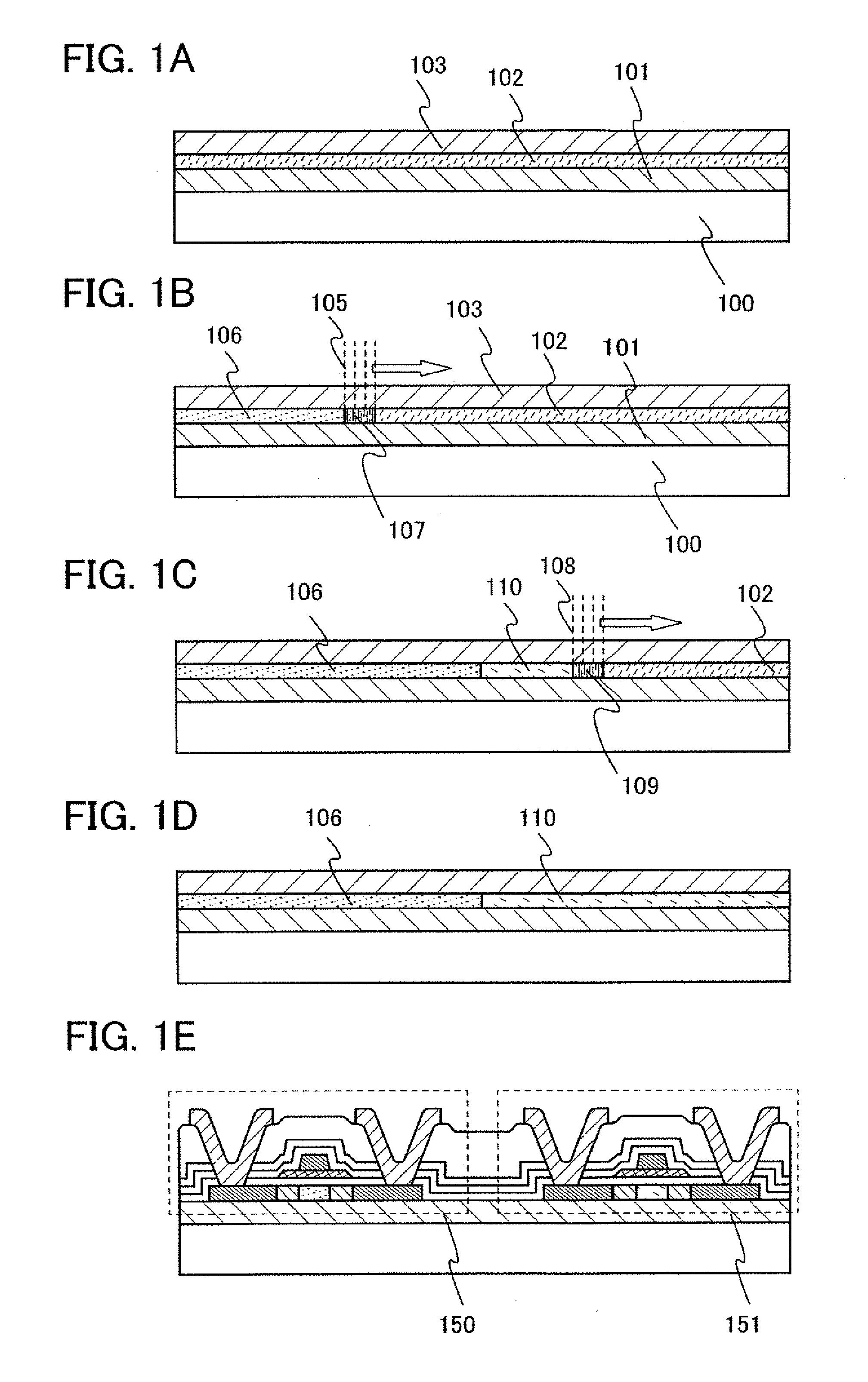
[0062]In this embodiment mode, a manufacturing method of a crystalline semiconductor film having crystals in which surface crystal planes are oriented along {100} and crystals in which crystal planes are oriented along {211} or {101}, in which a cap film is formed over an amorphous semiconductor film, and the amorphous semiconductor film is irradiated with a continuous-wave laser beam or a pulsed laser beam with a repetition rate of greater than or equal to 10 MHz, will be described with reference to FIGS. 1A to 1E and FIGS. 6 to 8.

[0063]First, as shown in FIG. 1A, an insulating film 101 functioning as a base film is formed on one surface of a substrate 100 with an insulating surface. The insulating film 101 functioning as a base film is formed using a silicon oxide film, a silicon nitride film, a silicon nitride oxide film in which the amount of nitrogen is larger than that of oxygen, a silicon oxynitride film in which the amount of oxygen is larger than that of nitrogen, or the li...

embodiment mode 2

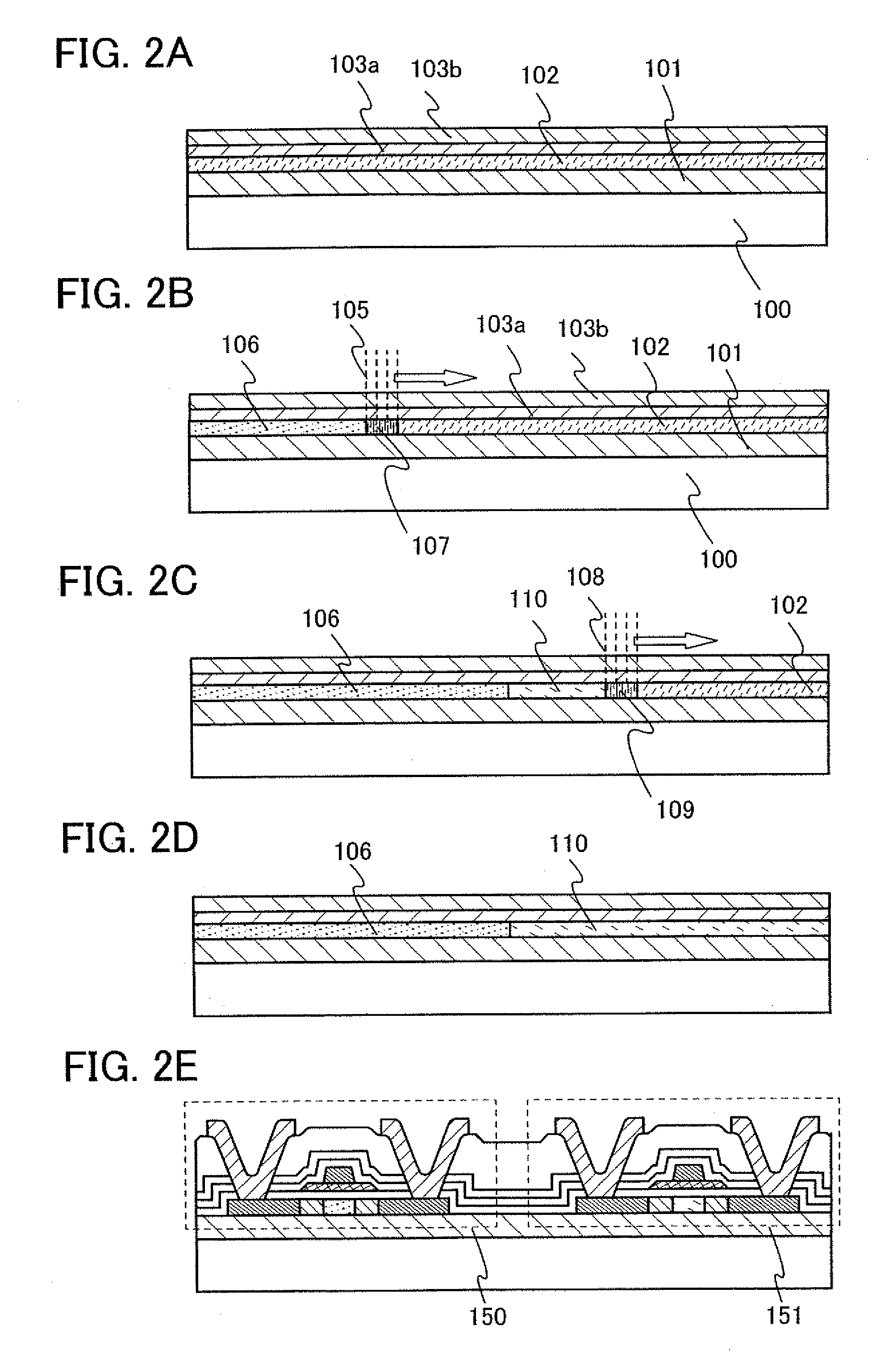
[0127]In this embodiment mode, a manufacturing method of a crystalline semiconductor film including a crystalline region in which crystal planes of the observation plane A are oriented along {001} and a crystalline region in which crystal planes of the observation plane A are oriented along {211} or {101} will be described with reference to FIGS. 2A to 2E.

[0128]In a similar manner to Embodiment Mode 1, as shown in FIG. 2A, an insulating film 101 functioning as a base film is formed on one surface of a substrate 100 with an insulating surface. Next, as a semiconductor film 102, an amorphous semiconductor film is formed to have a thickness of greater than or equal to 10 nm and less than or equal to 100 nm, preferably greater than or equal to 20 nm and less than or equal to 80 nm over the insulating film 101 by a plasma CVD method.

[0129]In addition, the semiconductor film 102 may be heated in an electric furnace at 500° C. for 1 hour after formation of the semiconductor film 102. In a ...

embodiment mode 3

[0143]In this embodiment mode, a manufacturing method of a crystalline semiconductor film including crystals in which crystal planes of the observation plane A are oriented along {001} and crystals in which crystal planes of the observation plane A are oriented along {211} or {101} due to a structure of a cap film which differs from that described in the above-described embodiment modes will be described with reference to FIGS. 3A to 3E.

[0144]In a similar manner to Embodiment Mode 1, as shown in FIG. 3A, an insulating film 101 functioning as a base film is formed on one surface of a substrate 100 with an insulating Surface. Next, as a semiconductor film 102, an amorphous semiconductor film is formed to have a thickness of greater than or equal to 10 nm and less than or equal to 100 nm, preferably greater than or equal to 20 μm and less than or equal to 80 nm over the insulating film 101 by a plasma CVD method.

[0145]In addition, the semiconductor film 102 may be heated in an electric...


PUM


Abstract

A cap film is formed over semiconductor films formed over an insulating substrate; the semiconductor films are irradiated with a laser beam which is capable of completely melting the semiconductor film in a film-thickness direction to completely melt the semiconductor film. By controlling the laser beam, a crystalline semiconductor films are formed over the substrate, in each of which orientations of crystal planes are controlled. In addition, an n-channel thin film transistor is formed using a crystalline region in which crystal planes are oriented along {001} and a p-channel thin film transistor is formed using a crystalline region in which crystal planes are oriented along {211} or {101}.

Description

BACKGROUND OF THE INVENTION[0001]1. Field of the Invention[0002]The present invention relates to a formation method of a semiconductor film having a crystalline structure which is formed by a laser crystallization technique, and a manufacturing method of a semiconductor device including a thin film transistor provided with the semiconductor film, or the like. More specifically, the present invention relates to a manufacturing method of a semiconductor device including an n-channel thin film transistor and a p-channel thin film transistor.[0003]2. Description of the Related Art[0004]In recent years, a laser crystallization technique in which an amorphous semiconductor film formed over a glass substrate is irradiated with a laser beam to form a semiconductor film having a crystalline structure (hereinafter, referred to as a crystalline semiconductor film) has been widely researched, and a large number of suggestions have been made.[0005]The reason why the crystalline semiconductor fil...

Claims


Application Information

Patent Timeline
Patent Type & Authority Applications(United States)
IPC IPC(8): H01L21/20
CPCH01L21/02532H01L21/02592H01L27/1285H01L27/1266H01L29/045H01L21/02691H01L27/1214
Inventor MORIWAKA, TOMOAKI
Owner SEMICON ENERGY LAB CO LTD
Why Eureka
Try Eureka