

Gan-Based III-V Compound Semiconductor Light-Emitting Element and Method for Manufacturing Thereof
a technology of compound semiconductors and light-emitting elements, which is applied in the direction of semiconductor devices, lasers, semiconductor lasers, etc., can solve the problems of reducing the reliability of semiconductor laser elements, deteriorating quality of active layers, and not being considered to have sufficient effectiveness, so as to achieve high light-emitting efficiency and reduce the generation of planar and linear crystal defects , the effect of high reliability
- Summary
- Abstract
- Description
- Claims
- Application Information
AI Technical Summary
Benefits of technology
Problems solved by technology
Method used
Image

Examples
example 1
PRACTICE EXAMPLE 1
Practice Example of GaN-Based III-V Group Compound Semiconductor Light-Emitting Element
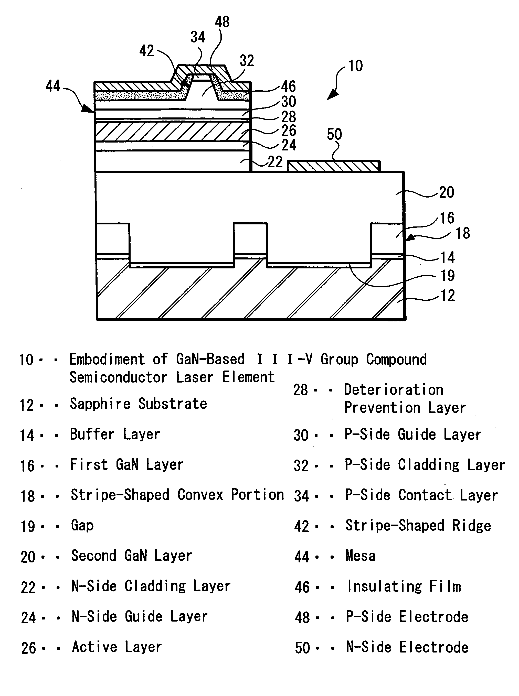
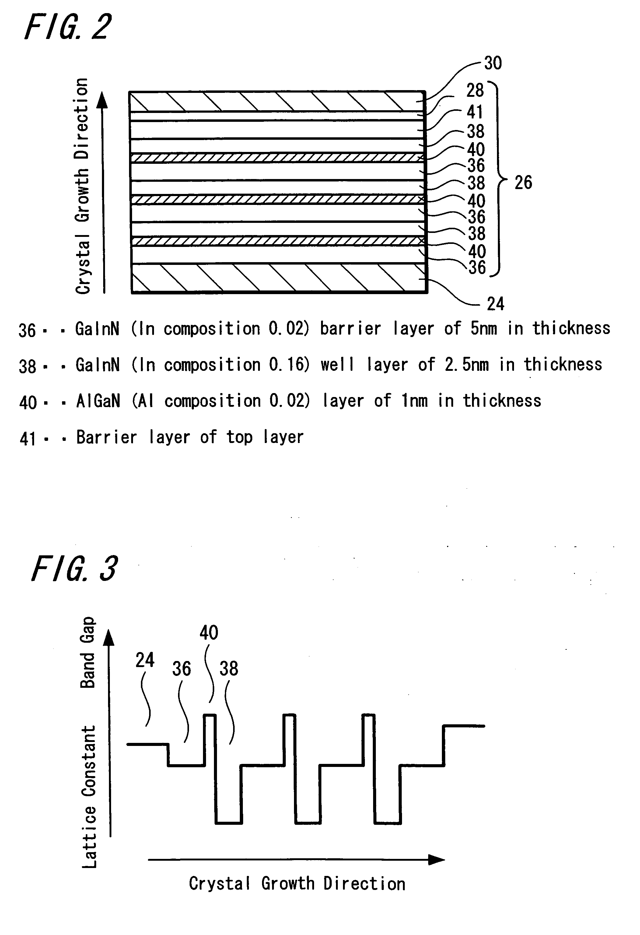
[0049]In this practice example, the GaN-based III-V group compound semiconductor light-emitting element according to the present invention is applied to a semiconductor laser element. FIG. 1 is a cross-sectional view showing a structure of the semiconductor laser element according to this practice example; FIG. 2 is a layer-construction view showing a structure of an active layer; and FIG. 3 is a view showing band gap energy of each layer constituting an active layer.
[0050]A GaN-based III-V group compound semiconductor laser element (hereinafter, referred to as a semiconductor laser element) 10 according to this practice example is, as shown in FIG. 1, a semiconductor laser element having an oscillation wavelength of 450 nm, in which a first GaN layer 16 having a thickness of 1 μm is laminated on a C-plane of a sapphire substrate 12 through a buffer layer 14 made of a GaN-based s...
example 2
PRACTICE EXAMPLE 2
Practice Example of Method for Manufacturing GaN-Based III-V Group Compound Semiconductor Light-Emitting Element
[0064]This practice example is an example in which a method for manufacturing the GaN-based III-V group compound semiconductor light-emitting element according to the present invention is applied to the manufacture of the semiconductor laser element 10 described in the above practice example. FIGS. 4A and 4B are cross-sectional views respectively showing main processes when a semiconductor laser element is manufactured in accordance with the method of this practice example.
[0065]In the manufacturing method according to this practice example, first, as shown in FIG. 4A, basically similarly to a method in the past, the undoped GaN buffer layer 14 is grown by a MOCDV method at a temperature of approximately 520° C. on the C-plane of the sapphire substrate 12 whose surface is cleaned up beforehand by using a thermal cleaning or the like. Then, an undoped firs...
example 3
PRACTICE EXAMPLE 3
[0084]In this practice example, instead of the active layer of the practice example 1 shown in FIG. 2, the active layer shown in FIG. 5 is used to form the semiconductor laser element 10 shown in FIG. 1.
[0085]As shown in FIG. 5, the active layer 26 includes a barrier layer 36 made of GaInN layer having a thickness of 5 nm and a well layer 38 made of GaInN layer having a thickness of 2.5 nm constituting a quantum well structure, and has a structure in which a combination of a planar crystal defect prevention layer 40 made of an AlGaN layer having a thickness of 1 nm respectively provided between the upper surface of the barrier layer 36 and the lower surface of the well layer 38 and between the upper surface of the well layer 38 and the lower surface of the barrier layer 36 is laminated once to several times and the top layer is terminated with a barrier layer 41 (a triple quantum well structure in this example). The barrier layer 41 of the top layer has the same co...
PUM
 Abstract
Description
Claims
Application Information