Method of manufacturing silicon carbide semiconductor device

a technology of silicon carbide and semiconductors, applied in the direction of semiconductor devices, basic electric elements, electrical equipment, etc., can solve the problems of reactive ion etching, inability to employ mass-productive trench formation, and almost limit properties of si power devices, so as to improve the corner shape and inner surface properties of trenches, high breakdown voltage, and high current flow

Inactive Publication Date: 2008-09-11
FUJI ELECTRIC CO LTD
View PDF10 Cites 61 Cited by
  • Summary
  • Abstract
  • Description
  • Claims
  • Application Information

AI Technical Summary

Benefits of technology

[0010]The present invention relates to a method of manufacturing a semiconductor device, particularly to a manufacturing method that facilitates to improve the corner shapes and inner surface ...

Problems solved by technology

However, since the Si semiconductor properties have already reached the extremes of improvements thereof, the Si power devices exhibit almost the limit properties due to the physical properties of the semiconductor Si.
Therefore, the reactive ion etching (hereinafter referred to as the “RIE”) used usually for forming trenches in a Si substrate is not employable for the mass-productive trench formation in the SiC substrate.
As compared with the trench shape control performed by the RIE in the Si substrate, it is not so easy for the dry etching to form trenches having a good profile in the SiC substrate.
It is also quite hard to provide the trench side wall with excellent smoothness only using dry etching.
The car...

Method used


Image

  • Method of manufacturing silicon carbide semiconductor device
  • Method of manufacturing silicon carbide semiconductor device
  • Method of manufacturing silicon carbide semiconductor device

Examples


Embodiment Construction

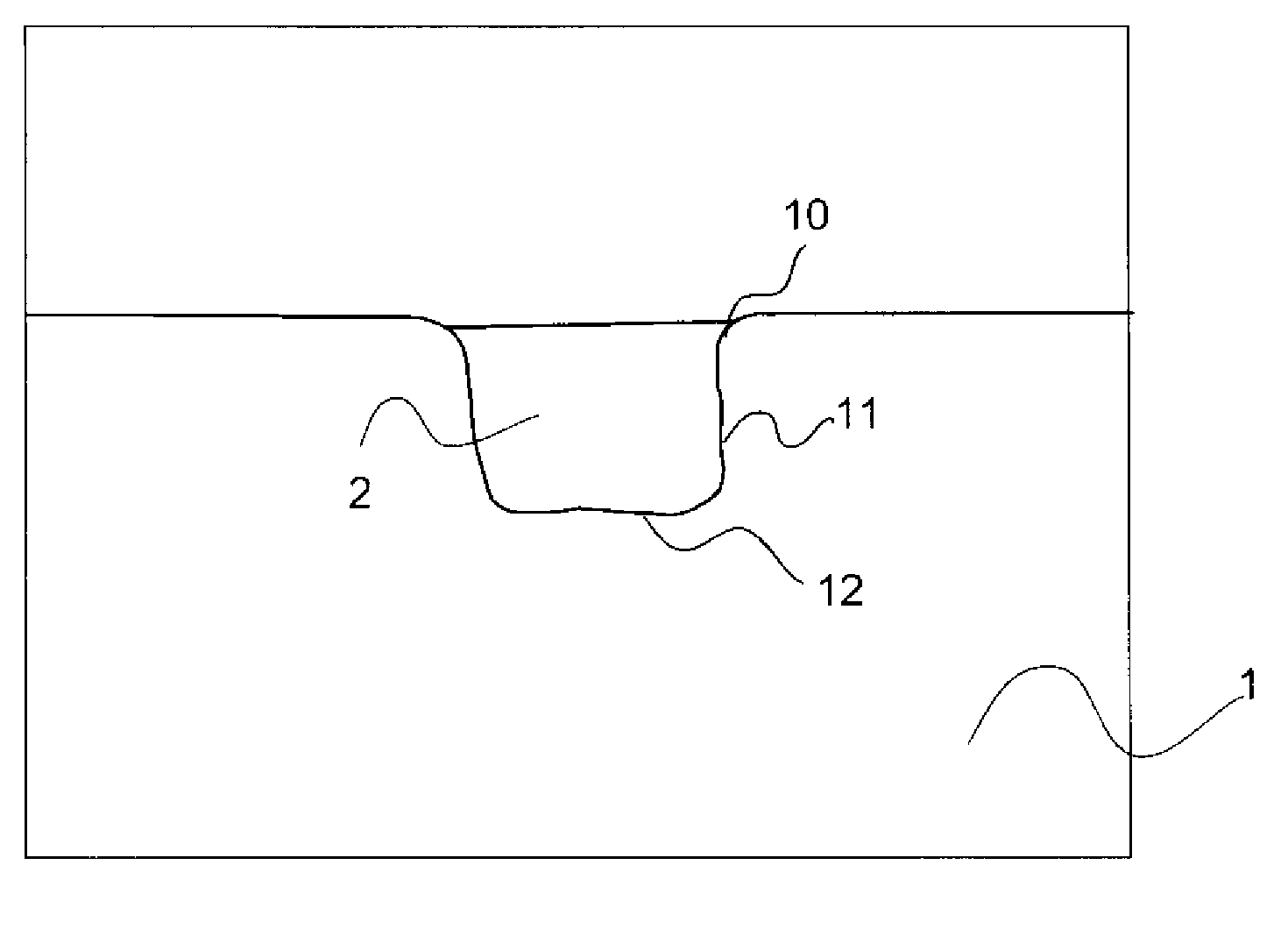
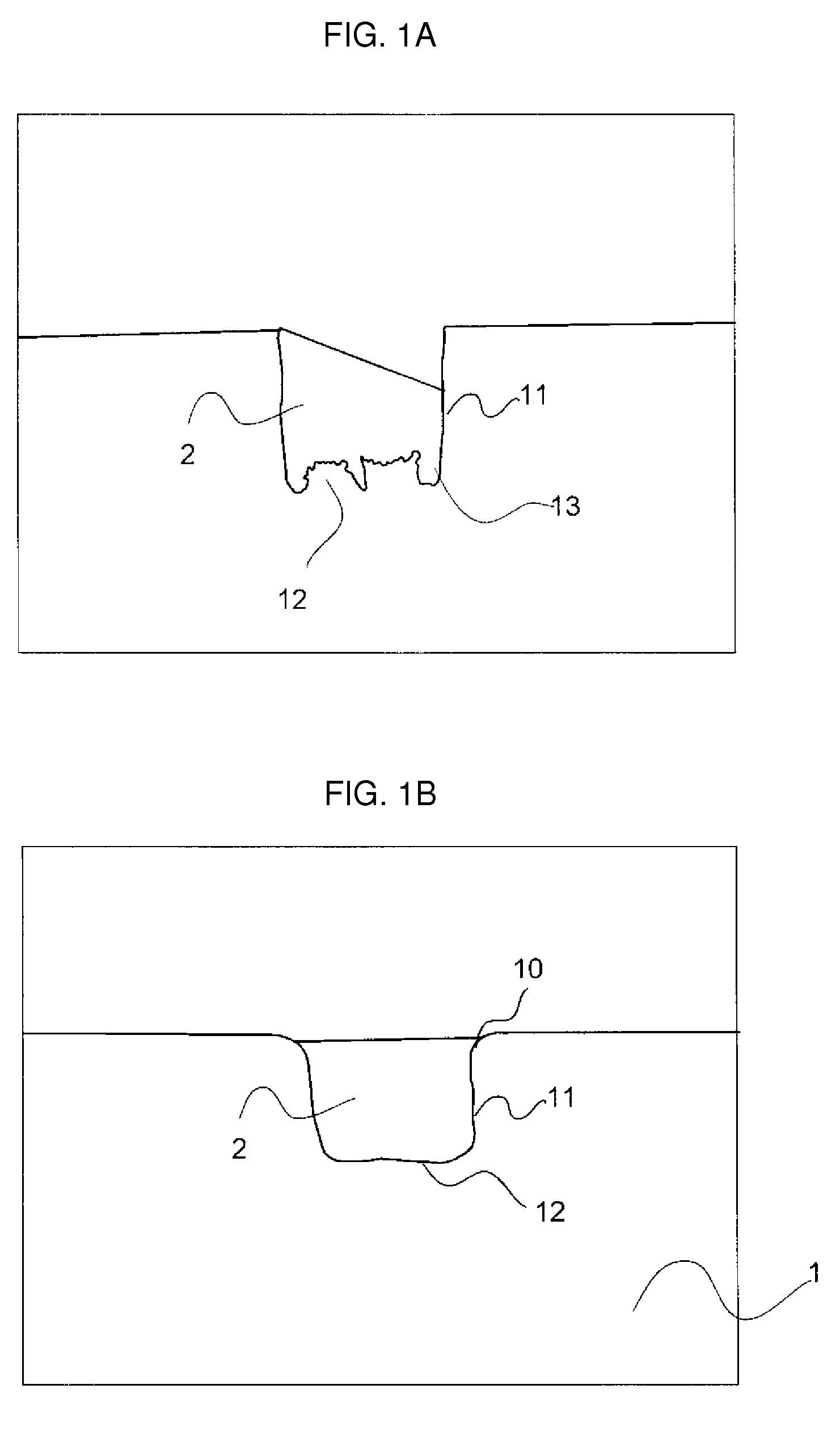
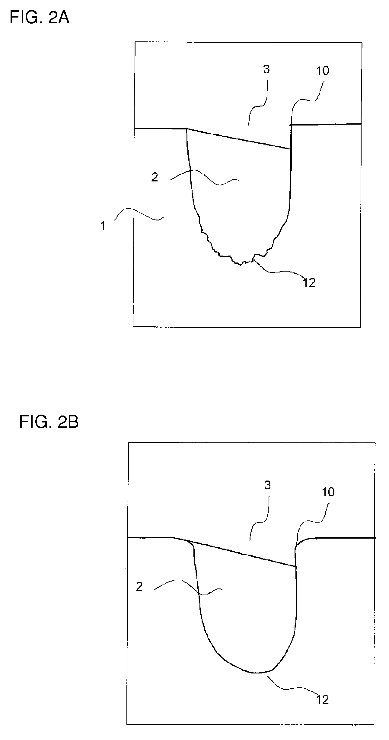
[0021]A method of manufacturing a semiconductor device according to the present invention follows in detail with reference to the accompanied drawings, which schematically illustrate the specific embodiments of a semiconductor device. In the drawings, numeral 1 denotes a SiC substrate, 2 denotes a trench, 3 denotes an opening, 4 denotes a substrate, 5 denotes an n-type SiC layer, 6 denotes a p-type SiC layer, 7 denotes an n-type source region, 8 denotes a p-type body contact region, 9 denotes a silicon oxide film, 10 denotes an edge corner of the trench opening, 11 denotes a trench side wall, 12 denotes a trench bottom, 13 denotes a sub-trench, 14 denotes aluminum, 15 denotes an Al ion implantation region, 16 denotes a gate insulating film, 17 denotes a gate, 18 denotes an interlayer insulating film, 19 denotes a source, and 20 denotes a drain.

[0022]The trench 2 is formed in the SiC substrate 1 by dry etching, and thereafter the internal surface shape and internal surface property o...


PUM


Abstract

A method of manufacturing a silicon carbide semiconductor device includes forming a trench for a MOS gate in an SiC substrate by dry etching. Thereafter, the substrate with the trench is heat treated. The heat treatment includes heating the substrate in an Ar gas atmosphere or in a mixed gas atmosphere containing SiH4 and Ar at a temperature between 1600° C. and 1800° C., and thereafter in a hydrogen gas atmosphere at a temperature between 1400° C. and 1500° C. The present manufacturing method smoothens the trench inner surface and rounds the corners in the trench to prevent the electric field from localizing thereto.

Description

BACKGROUND[0001]Semiconductor power devices, including a MOSFET power device and an IGBT power device, which employ silicon (hereinafter referred to sometimes as “Si”) for the semiconductor material thereof, are devices typically used in inverters and apparatuses for electric power control. However, since the Si semiconductor properties have already reached the extremes of improvements thereof, the Si power devices exhibit almost the limit properties due to the physical properties of the semiconductor Si.[0002]In contrast, since silicon carbide (hereinafter referred to as “SiC”) exhibits excellent physical properties as described below, SiC (4H—SiC) is more advantageous than Si especially for the power device material. The electric field strength that causes a dielectric breakdown in SiC is 10 times as high as the electric field strength that causes a dielectric breakdown in Si. The band gap in SiC is 2.9 times as wide as the band gap in Si. The thermal conductivity in SiC is 3.2 ti...

Claims


Application Information

Patent Timeline
IPC IPC(8): H01L21/02
CPCH01L21/0475H01L21/049H01L21/3247H01L29/7813H01L29/1608H01L29/66068H01L29/0623
Inventor KAWADA, YASUYUKITAWARA, TAKESHITAWARA, TAE
Owner FUJI ELECTRIC CO LTD
Why Eureka
Try Eureka