Gate dielectric structures, organic semiconductors, thin film transistors and related methods

Inactive Publication Date: 2008-09-18
NORTHWESTERN UNIV
View PDF7 Cites 16 Cited by
  • Summary
  • Abstract
  • Description
  • Claims
  • Application Information

AI Technical Summary

Benefits of technology

[0015]As illustrated below, this invention can also be directed to a method of using a dielectric polymer coating to affect charge mobility of an organic semiconductor component or one or more thin film transistor parameters. Such a method can comprise fabricating a thin film transistor device comprising an inorganic dielectric component and an organic semiconductor component; and coupling an insulating organic polymer component to the inorganic dielectric component. Choice of such an organic polymer, in

Problems solved by technology

It is generally accepted that gate dielectric surface roughness is an important parameter affecting OTFT electrical performance, and it was shown that rougher gate dielectric surfaces result in smaller pentacene grains and lower OTFT carrier mobilities.
Although these results demonstrate the importance of controlling fundamental dielectric and/or interfacial properties for optimizing/controlling OSC

Method used


Image

  • Gate dielectric structures, organic semiconductors, thin film transistors and related methods
  • Gate dielectric structures, organic semiconductors, thin film transistors and related methods
  • Gate dielectric structures, organic semiconductors, thin film transistors and related methods

Examples


example 1a

Bilayer Dielectric Fabrication and Characterization

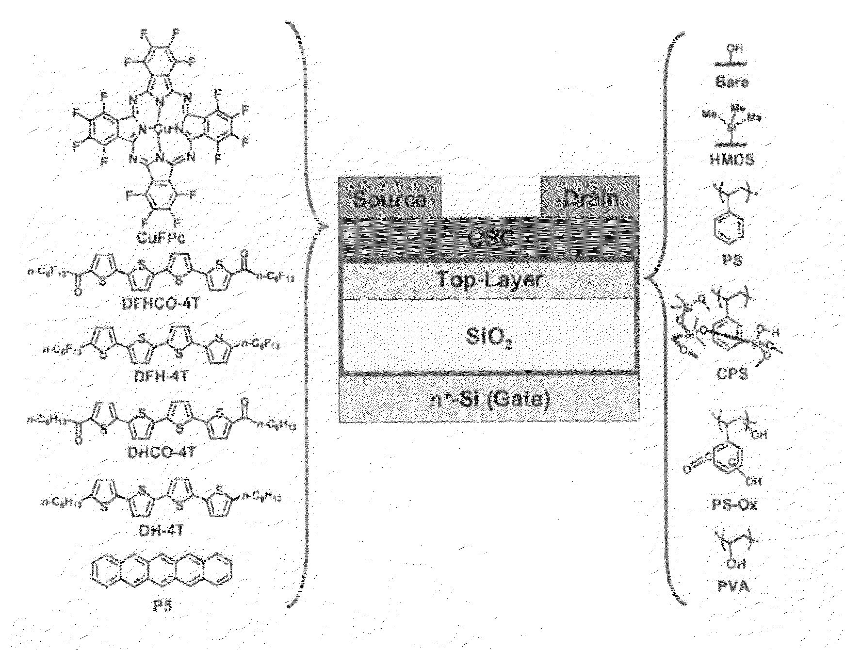
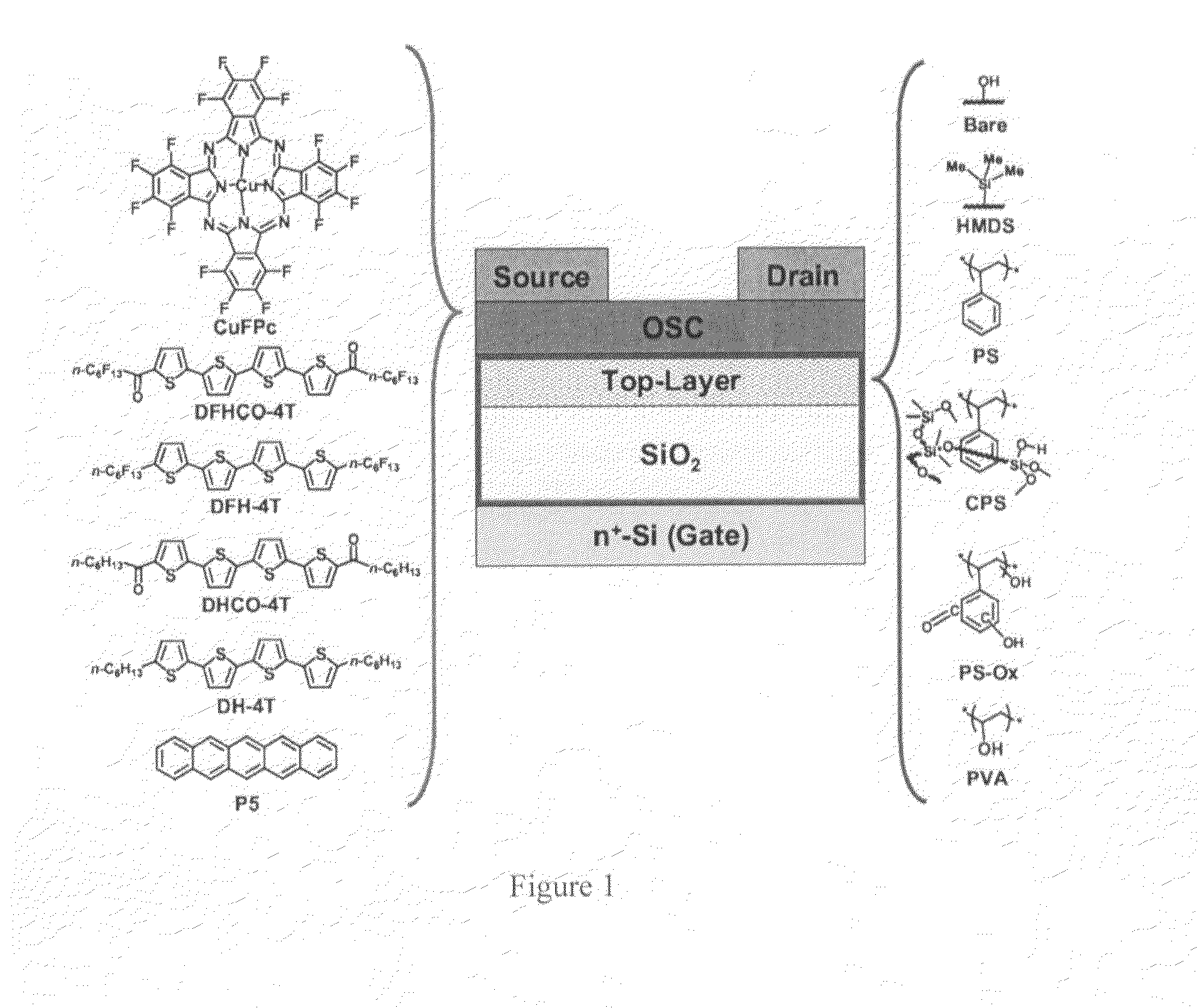
[0068]All of the bilayer dielectric samples were fabricated on p+-Si / SiO2 (300 nm) substrates. The top polymer layer was deposited by spin-coating according to the procedure described above. The polymers employed in this study are polystyrene (PS), a crosslinked polystyrene blend (CPS), and polyvinyl alcohol (PVA). Therefore, the following dielectric structures were fabricated / investigated and are identified here as the following (FIG. 1, right): are, p+-Si / SiO2 (300 nm) treated with O2 plasma before use; HMDS, p+-Si / SiO2 (300 nm) treated with HMDS vapor before use; PS1, p+-Si SiO2 (300 nm) / PS (24 nm); PS2, p+-Si / SiO2 (300 nm) / PS (31 nm); PS3, p+-Si / SiO2 (300 nm) / PS (71 nm); PS4, p+-Si / SiO2 (300 nm) / PS (150 nm); PS-Ox, p+-Si / SiO2 (300 nm) / PS (24 nm) treated with O2 plasma; CPS, p+-Si / SiO2 (300 nm) / CPS (13 nm); PVA, p+-Si / SiO2 (300 nm) / PVA (115 nm). These samples allow investigating the effects of a wide range of surface energies, as...

example 1b

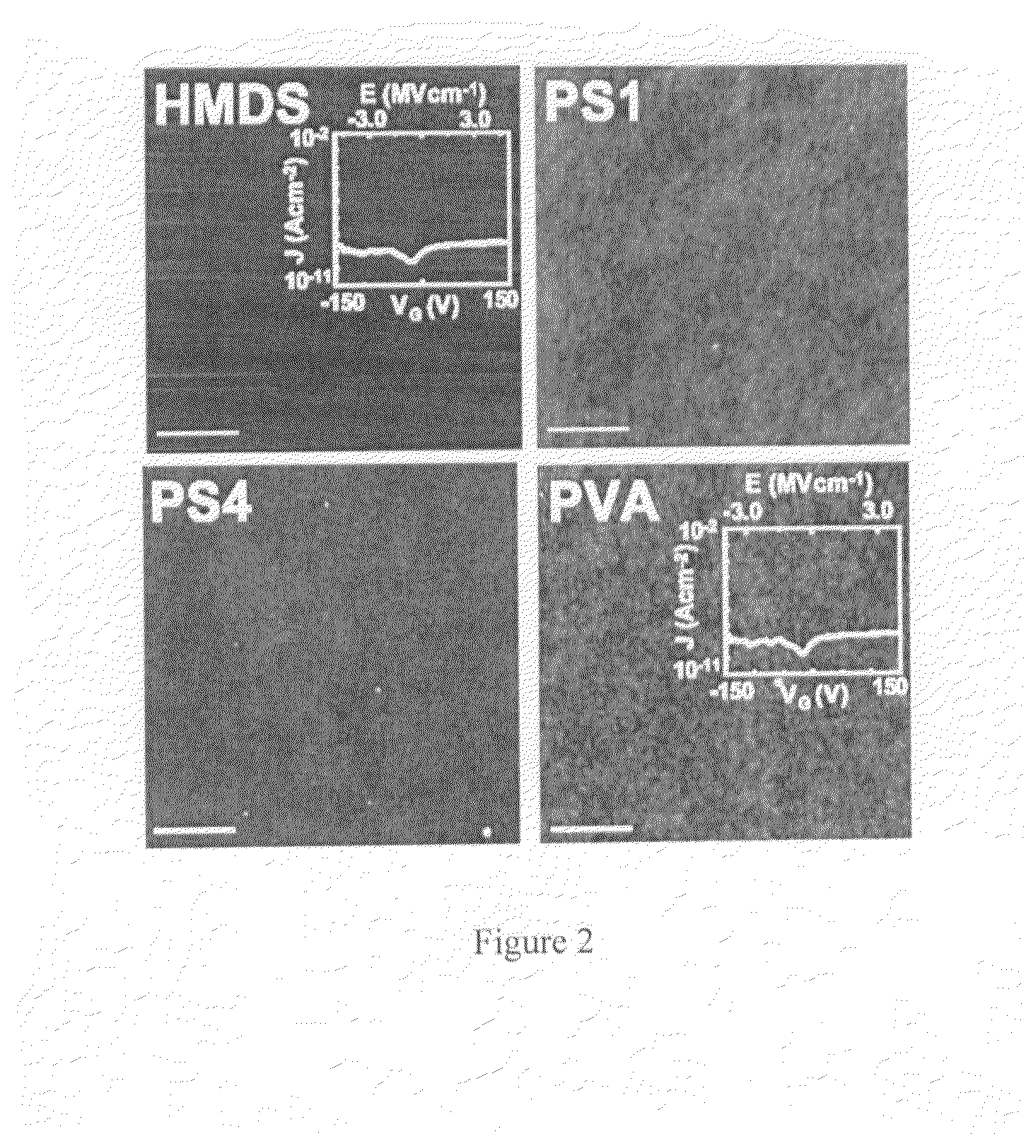
[0069]Typical leakage current densities of the surface-modified substrates are identical to that of pristine p+-Si / SiO2 (Bare), −9A / cm2 at E˜4 MV / cm, as measured in MIS structures (M=Au, 200×200 μm contact area). The insets of the AFM images in FIG. 2 show that the current density versus voltage plots for the thinnest (Bare,) and the thickest (PS4) insulators are identical. This result demonstrates that the leakage current densities at the maximum OTFT gate fields employed here (˜3.3 MV / cm) are dominated by the bottom SiO2 layer. AFM micrographs of the bilayer films reveal that with the exception of CPS (RMS roughness ρ˜0.9 nm), all dielectric samples exhibit very similar topographies characterized by very smooth AFM morphologies with ρ=0.1˜0.3 nm, slightly larger for the thicker PSn films (Table 3). Representative AFM images are also shown in FIG. 2. Consequently, the differences among OTFT performance parameters (vide infra) can be mainly attributed to the chemical nature of the d...

example 2a

Thin-Film Transistor Fabrication and Characterization

[0071]As discussed above, studies on OTFTs fabricated with bilayer dielectrics (and most of those using a single polymer dielectric layer) have been limited to pentacene devices. With the goal of more fully understanding structure-property relationships governing diverse organic semiconductor-dielectric interfaces, the OTFT performance characteristics of six semiconductors on nine bilayer dielectrics were analyzed. The semiconductors investigated here (FIG. 1, left) were selected to span all possible combinations of majority carrier transport type observed on untreated / HMDS-functionalized SiO2 dielectrics and are: i) N-type. Perfluoro-copperphthalocyanine (CuFPc), α,ω-diperfluorohexylcarbonyl-quaterthiophene (DFHCO-4T), and α,ω-diperfluorohexylquaterthiophene (DFH-4T); ii) Ambipolar. α,ω-Dihexylcarbonyl-quaterthiophene (DHCO-4T); iii) P-type. α,ω-Dihexylcarbonyl-quaterthiophene (DH-4T) and pentacene (P5) (FIG. 1). Pentacene was in...


PUM

PropertyMeasurementUnit
Fractionaaaaaaaaaa
Areaaaaaaaaaaa
Areaaaaaaaaaaa

Abstract

Gate dielectric structures comprising an organic polymeric component, and organic semiconductor components, as can be used to fabricate thin film transistor devices.

Description

[0001]This application claims priority benefit from provisional application Ser. No. 60 / 839,383 filed on Aug. 22, 2006, the entirety of which is incorporated herein by reference.[0002]The United States government has certain rights to this invention pursuant to grant nos. STTR FA9550-05-C-0167, DMR-0076097, NCC 2-1363 and N00014-02-1-0909 from the AFOSR, NSF, NASA Institute for Nanoelectronics and Computing, and ONR, respectfully, to Northwestern University.BACKGROUND OF THE INVENTION[0003]Field-effect-active organic semiconductors (OSCs) are of great interest for use in low-cost / disposable electronic products such as smart cards and radio frequency identification (RFID) tags, as well as in flexible display driver circuits, nonvolatile memories, and sensors. Indeed, amorphous and polycrystalline films of several OSCs exhibit hole or electron carrier mobilities comparable to or surpassing those of the inorganic semiconductor typically used for the aforementioned applications: amorpho...

Claims


Application Information

Patent Timeline
IPC IPC(8): H01L51/40H01L51/00
CPCH01L51/0036H01L51/0533H01L51/0068H10K85/113H10K85/655H10K10/476
Inventor MARKS, TOBIN J.FACCHETTI, ANTONIOYOON, MYUNG-HAN
Owner NORTHWESTERN UNIV
Why Eureka
Try Eureka