STRUCTURE AND METHOD FOR SiCOH INTERFACES WITH INCREASED MECHANICAL STRENGTH

a technology of mechanical strength and structure, applied in the direction of resistive material coating, solid-state device, chemical vapor deposition coating, etc., can solve the problems of reducing the reliability of mechanical response, dicing into chips, and increasing signal delays in ulsi electronic devices, so as to improve the interfacial strength between different layers

Active Publication Date: 2008-09-25
IBM CORP +1
View PDF16 Cites 29 Cited by
  • Summary
  • Abstract
  • Description
  • Claims
  • Application Information

AI Technical Summary

Benefits of technology

[0012]The purposes and advantages of the invention have been achieved by providing, according to a first aspect of the invention, a method for improving the interfacial strength between different layers, the method comprising the steps of:

Problems solved by technology

This combined effect increases signal delays in ULSI electronic devices.
The adhesion among the different layers in the complex structures of an IC device is often too low, resulting in delaminations during the processing of the device, dicing into chips, or reduced reliability in response to mechanical stresses imposed by typical chip packaging materials.
Often even when the adhesion is adequate, the deposited low-k film may possess degraded cohesive strength near the initial interface that is formed during deposition, and adhesion testing leads to fracture within this initial layer, which may be from single to tens of nm thick.
Without careful failure analysis, the low failure energies from adhesion testing of such cases may be mistakenly attributed to poor interfacial adhesion, rather than substandard cohesive strength of the near-interface low-k film.
The present inventors have found that porous dielectric layers present certain difficulties in their formation, particularly due to the carbon generated by the porogen used to form the pores in the dielectric.
Another difficulty arises when the precursors used to form porous dielectric layers react rapidly in the gas phase, forming particulates which settle on the manufacturing substrate, an occurrence known as gas phase nucleation (GPN).
Particles then cause patterning defects and other manufacturing failures.

Method used


Image

  • STRUCTURE AND METHOD FOR SiCOH INTERFACES WITH INCREASED MECHANICAL STRENGTH
  • STRUCTURE AND METHOD FOR SiCOH INTERFACES WITH INCREASED MECHANICAL STRENGTH
  • STRUCTURE AND METHOD FOR SiCOH INTERFACES WITH INCREASED MECHANICAL STRENGTH

Examples


example 1

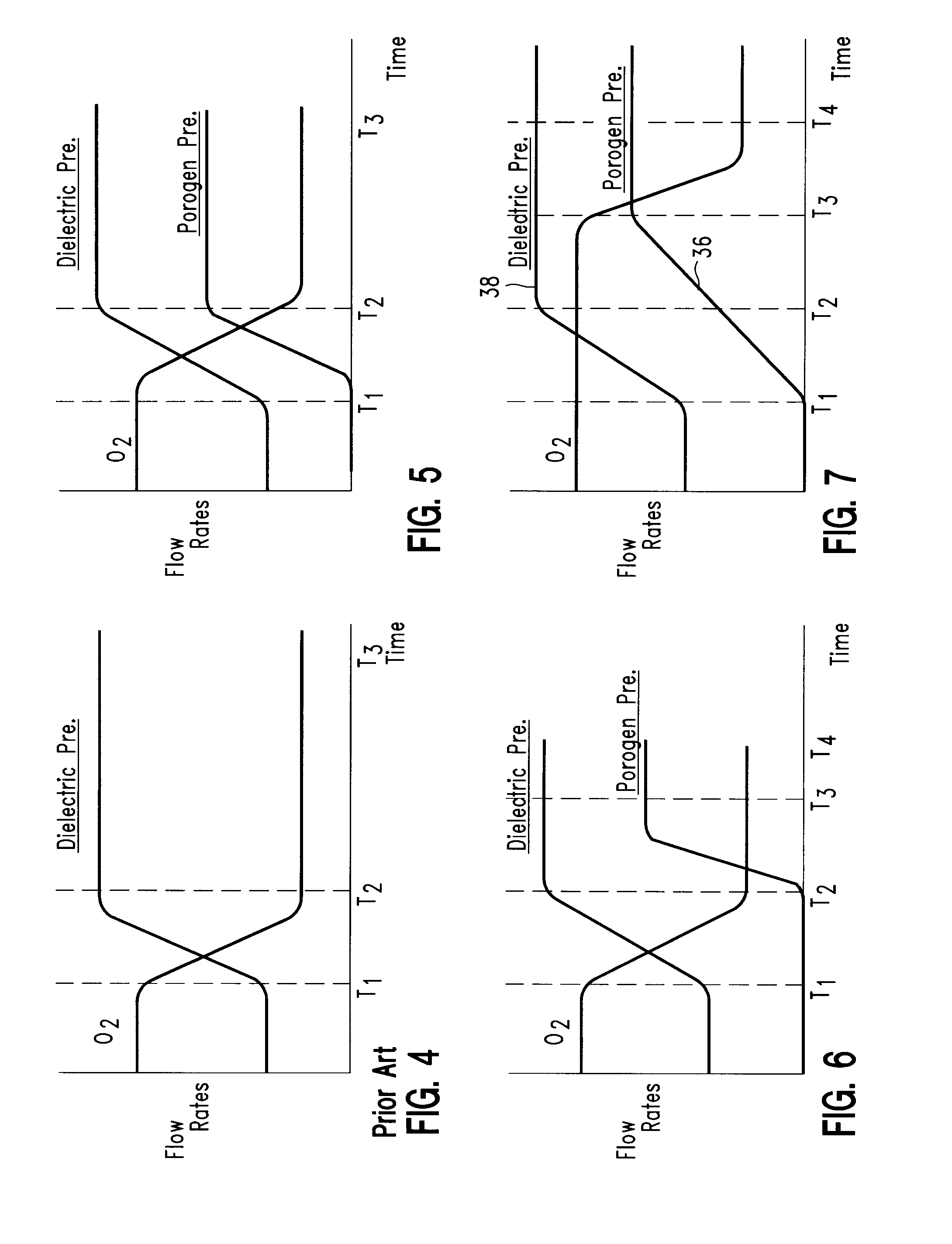
[0071]A Si wafer containing a layer of SiCNH alloy was used to simulate an interconnect substrate with the same SiCNH alloy capping a pre-formed patterned interconnect layer. A Si wafer containing a layer of SiCNH alloy was placed in a PECVD chamber and a porous SiCOH layer was prepared according to the flow rates of oxygen, dielectric precursor and porogen precursor illustrated in FIG. 5. Particulars of the process are described in the following Table 1.

TABLE 1Step Label in Figure0 to T1T1 to T2T3Duration (seconds)1 to 41 to 430 to 60RF Power, GeneralLowHighHighDescriptionExample RF Power (W)300–500600–700600–700Dielectric Precursor FlowLowRamping Low toHighHighPorogen precursor FlowZeroRamping to HighHighO2 FlowHighLowLow

[0072]A TOF-SIMS analysis was done of the completed structure. The result is illustrated in FIG. 9.

[0073]The X axis of FIG. 9 is the sputter time, which is proportional to depth into the sample with zero of the X axis being the top surface of the sample and the ti...

example 2

[0075]A second Si wafer containing a layer of SiCNH alloy (simulating an interconnect substrate) was placed in a PECVD chamber and a porous SiCOH formed according to the flow rate profiles of oxygen, DEMS dielectric precursor and BCHD porogen precursor as illustrated in FIG. 6. The particulars of the process are illustrated in Table 2 below.

TABLE 2Step Label in Figure0 to T1T1 to T2T2 to T3T4Duration (seconds)1 to 41 to 41 to 430 to 60RF Power, GeneralLowHighHighHighDescriptionExample RF Power (W)300–500600–700600–700600–700Dielectric PrecursorLowRampingHighHighFlowLow toHighPorogen precursor FlowZeroZeroRampingHighto HighO2 FlowHighLowLowLow

[0076]It was found advantageous by the inventors to decrease the power density of the plasma such that steps 0 to T2 are performed with a reduced power density and steps after T2 are performed with a higher power density. It was found advantageous by the inventors that a SiCOH precursor ramp rate between 500 to 1500 milligrams per minute / second ...

example 3

[0078]A third interconnect substrate was prepared by placing the substrate in a PECVD chamber and flowing oxygen, DEMS dielectric precursor and BCHD porogen precursor according to the flow rate profile illustrate in FIG. 7. The particulars of the process are illustrated in Table 3 below.

TABLE 3Step Label in Figure0 to T1T1 to T2T2 to T3T4Duration (seconds)1 to 41 to 4430 to 60RF Power, GeneralLowHighHighHighDescriptionExample RF Power (W)300–500600–700600–700600–700Dielectric Precursor FlowLowRampingHighHighLow toHighPorogen precursor FlowZeroRampingRampingHighto Highto HighO2 FlowHighHighHighLow

[0079]It was found advantageous by the inventors to decrease the power density of the plasma such that steps 0 to T2 are performed with a reduced power density and steps after T2 are performed with a higher power density. It was found advantageous by the inventors that a SiCOH precursor ramp rate between 500 to 1500 milligrams per minute / second and a porogen precursor ramp rate between 100 t...


PUM

PropertyMeasurementUnit
dielectric constantaaaaaaaaaa
thicknessaaaaaaaaaa

Abstract

Disclosed is a structure and method for forming a structure including a SiCOH layer having increased mechanical strength. The structure includes a substrate having a layer of dielectric or conductive material, a layer of oxide on the layer of dielectric or conductive material, the oxide layer having essentially no carbon, a graded transition layer on the oxide layer, the graded transition layer having essentially no carbon at the interface with the oxide layer and gradually increasing carbon towards a porous SiCOH layer, and a porous SiCOH (pSiCOH) layer on the graded transition layer, the porous pSiCOH layer having an homogeneous composition throughout the layer. The method includes a process wherein in the graded transition layer, there are no peaks in the carbon concentration and no dips in the oxygen concentration.

Description

BACKGROUND OF THE INVENTION[0001]The present invention generally relates to a semiconductor electronic device structure comprising at least one porous SiCOH (pSiCOH, carbon-doped oxide) layer having improved interfacial strength (adhesive and cohesive strength near the interface) to a dielectric or conducting layer. The improved interfacial strength is caused by the presence of transition layers that are formed between the porous SiCOH layer and the dielectric or conducting layer. The transition layers are formed in the present invention by starting the deposition of a specific layer, while a surface preparation plasma is still present and active in the reactor.[0002]The continuous shrinking in dimensions of electronic devices utilized in ULSI circuits in recent years has resulted in increasing the resistance of the BEOL metallization without concomitantly decreasing the interconnect capacitances. Often interconnects are even scaled to higher aspect ratios to mitigate the resistance...

Claims


Application Information

Patent Timeline
Patent Type & Authority Applications(United States)
IPC IPC(8): B32B3/00B05D5/12
CPCC23C16/0272C23C16/029C23C16/401H01L21/02126H01L21/02203H01L21/02216Y10T428/24851H01L21/02304H01L21/31695H01L21/7682H01L21/76832H01L21/76834H01L21/76835H01L21/02274H01L2221/1047Y10T428/249961H01L21/4763
Inventor EDELSTEIN, DANIEL C.DEMOS, ALEXANDROSGATES, STEPHEN M.GRILL, ALFREDMOLIS, STEVEN E.NGUYEN, VU NGOC TRANREITER, STEVENRESTAINO, DARRYL D.YIM, KANG SUB
Owner IBM CORP
Why Eureka
Try Eureka