Method For The Simultaneous Grinding Of A Plurality Of Semiconductor Wafers

Active Publication Date: 2008-09-25
PETER WOLTERS GMBH
View PDF22 Cites 54 Cited by
  • Summary
  • Abstract
  • Description
  • Claims
  • Application Information

AI Technical Summary

Benefits of technology

[0020]It is an object of the present invention, therefore, to provide semiconductor wafers which, on account of their geometry, are also suitable for producing electronic components with very small linewidths (“design rules”). In particular, the object was established to avoid geometrical faults such as a thickness maximum in the center of the semiconductor wafer associated with a continuously decreasing thickness toward the edge of the wafer, an edge roll-off, or a local thickness minimum in the center of the semiconductor wafer. A further object was to avoid excessive surface roughness or damage of the semiconductor wafer. In particular, an object was to produce a semiconductor wafer with low bow and warp. A still further object w

Problems solved by technology

This is because interruptions for possibly required setting, truing or dressing processes or frequently required tool changes lead to unpredictable “cold start” influences which nullify the desired features of the methods, and adversely affect the economic viability.
Lapping produces a very high damage depth and surface roughness on account of the brittle-erosive material removal as a result of the rolling movement of the loosely supplied lapping grain.
This necessitates complicated subsequent machining for removing these damaged surface layers, whereby the advantages of lapping are nullified again.
Moreover, as a result of depletion and loss of sharpness of the supplied grain during transport from the edge to the center of the semiconductor wafer, lapping always yields semiconductor wafers having a disadvantageously convex thickness profile with wafer edges of decreasing thickness (“edge roll-off” of the wafer thickness).
It has been found, however, that the semiconductor wafers machined by this method have a series of defects, with the result that the semiconductor wafers obtained are unsuitable for particularly demanding applications: it has thus been shown, for example, that in general semiconductor wafers result which have a disadvantageous convex thickness profile with a pronounced edge roll-off.
The semiconductor wafers often also have irregular undulations in their thickness profile and also a rough surface with a large damage depth.
The high damage depth necessitates complicated subsequent machining that nullifies the advantage of the method disclosed in DE10344602A1.
The remaining convexity a

Method used


Image

  • Method For The Simultaneous Grinding Of A Plurality Of Semiconductor Wafers
  • Method For The Simultaneous Grinding Of A Plurality Of Semiconductor Wafers
  • Method For The Simultaneous Grinding Of A Plurality Of Semiconductor Wafers

Examples


first embodiment

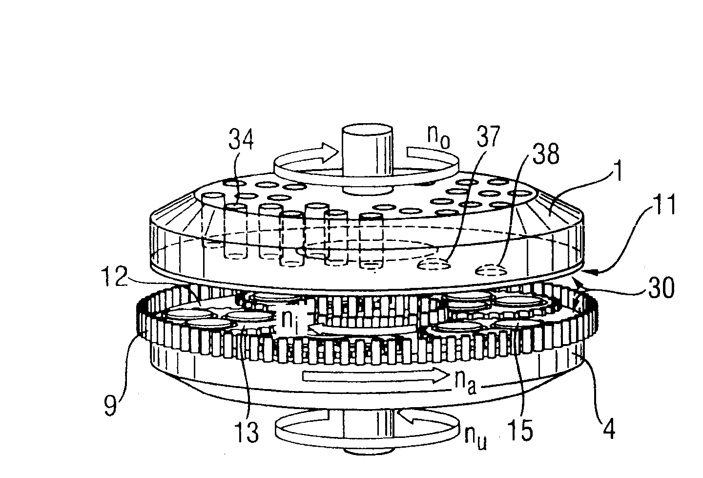
[0203]For this third method according to the invention (carrier with little interaction), use is made of a carrier which is completely composed of a first material or bears a full or partial coating composed of a first material such that only this layer comes into contact with the working layer during the machining, said first material having a high abrasion resistance.

[0204]Polyurethane (PU), polyethylene terephthalate (PET), silicone, rubber, polyvinyl chloride (PVC), polyethylene (PE), polypropylene (PP), polyamide (PA) and polyvinyl butyral (PVB), epoxy resin and phenolic resins are preferred for said first material. Furthermore, polycarbonate (PC), polymethyl methacrylate (PMMA), polyether ether ketone (PEK), polyoxymethylene / polyacetal (PON), polysulfone (PSU), polyphenylene sulfone (PPS) and polyethylene sulfone (PES) can also advantageously be used.

[0205]Polyurethanes in the form of thermoplastic elastomers (TPE-U) are particularly preferred. Likewise particularly preferred ...

second embodiment

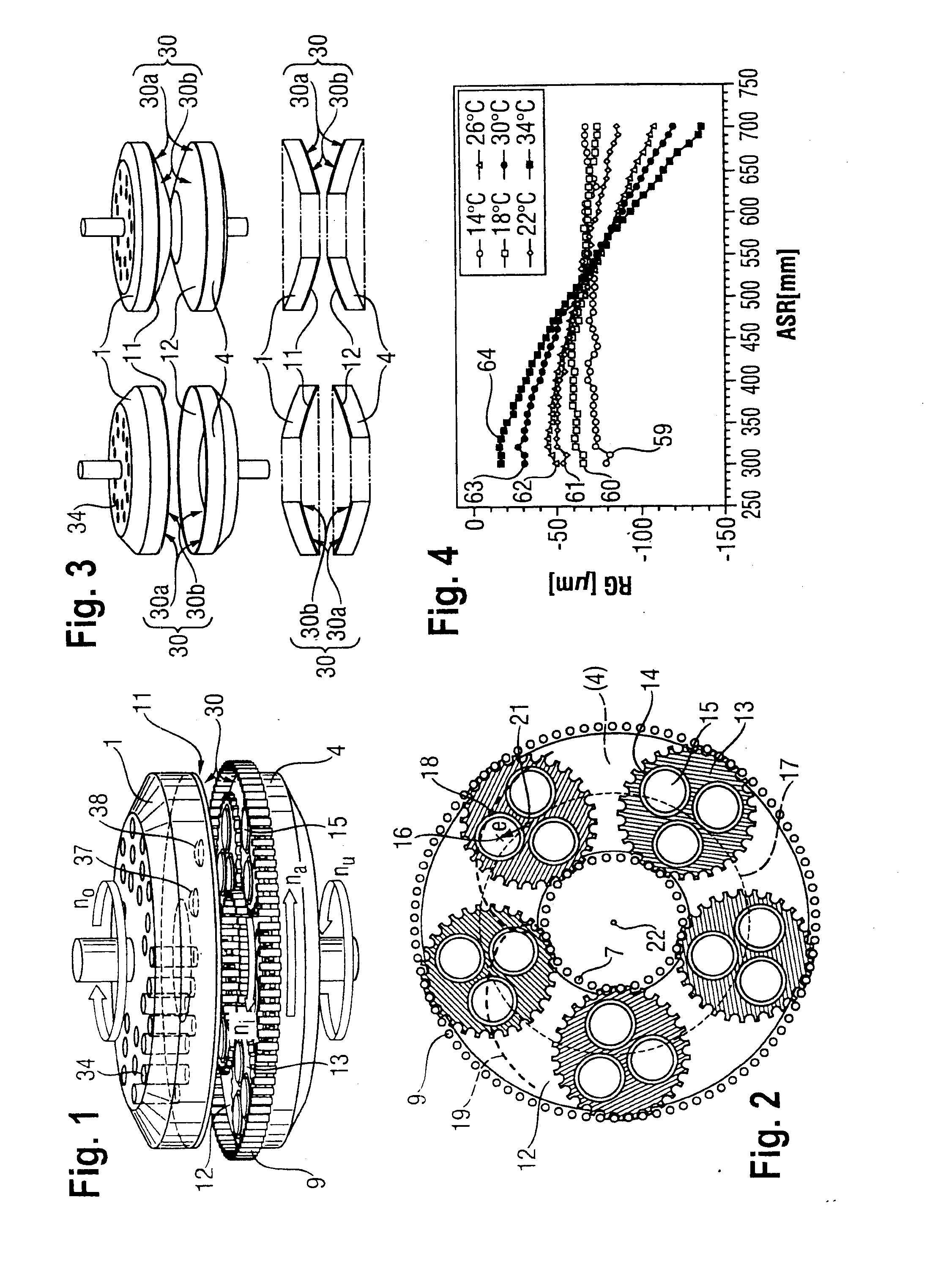
[0224]For the third method according to the invention (“dressing carrier”), use is made of a carrier which is completely composed of a second material or as a coating of the parts which come into contact with the working layer composed of a second material, said second material containing substances which dress the working layer.

[0225]It is preferred for said second material to contain hard substances and to be subject to wear upon contact with the working layer, such that hard substances that dress the working layer are released as a result of the wear. It is particularly preferred for the hard substances released in the course of the wear of the second material to be softer than the abrasive contained in the working layer. It is particularly preferred for the released material to be corundum (Al2O3), silicon carbide (SiC), zirconium oxide (ZrO2), silicon dioxide (SiO2) or cerium oxide (CeO2) and for the abrasive contained in the working layer to be diamond. Most preferably, the ha...


PUM

PropertyMeasurementUnit
Fractionaaaaaaaaaa
Fractionaaaaaaaaaa
Fractionaaaaaaaaaa

Abstract

Simultaneous double-side grinding of a plurality of semiconductor wafers involves positioning each wafer freely in a cutout of one of plural carriers which rotate on a cycloidal trajectory, wherein the wafers are machined between two rotating ring-shaped working disks, each disk having a working layer of bonded abrasive, wherein the form of the working gap between working layers is determined during grinding and the form of the working area of at least one disk is altered such that the gap has a predetermined form. The wafers, during machining, may temporarily overhang the gap. The carrier is optionally composed only of a first material, or is completely or partly coated with the first material such that during machining only the first material contacts the working layer, and the first material does not reduce the machining ability of the working layer.

Description

BACKGROUND OF THE INVENTION[0001]1. Field of the Invention[0002]The present invention relates to a method for the simultaneous double-side grinding of a plurality of semiconductor wafers, wherein each semiconductor wafer lies such that it is freely moveable in a cutout of one of a plurality of carriers caused to rotate by means of a rolling apparatus and is thereby moved on a cycloidal trajectory, wherein the semiconductor wafers are machined in material-removing fashion between two rotating ring-shaped working disks, wherein each working disk comprises a working layer containing bonded abrasive.[0003]2. Background Art[0004]Electronics, microelectronics and microelectromechanics require as starting materials (substrates) semiconductor wafers with extreme requirements made of global and local flatness, single-side-referenced local flatness (nanotopology), roughness, cleanness and freedom from impurity atoms, in particular metals. Semiconductor wafers are wafers made of semiconductor ...

Claims


Application Information

Patent Timeline
IPC IPC(8): B24B1/00B24B37/08B24B37/12B24B37/28
CPCB24B37/08B24B37/28B24B37/12H01L21/304
Inventor PIETSCH, GEORGKERSTAN, MICHAELAUS DEM SPRING, HEIKO
Owner PETER WOLTERS GMBH
Why Eureka
Try Eureka