

Isolated bipolar transistor
a bipolar transistor and isolation technology, applied in the direction of transistors, semiconductor devices, electrical equipment, etc., can solve the problems of not facilitating complete electrical isolation, unable to facilitate and unable to achieve complete electrical isolation of its fabricated devices
- Summary
- Abstract
- Description
- Claims
- Application Information
AI Technical Summary
Problems solved by technology
Method used
Image

Examples
Embodiment Construction
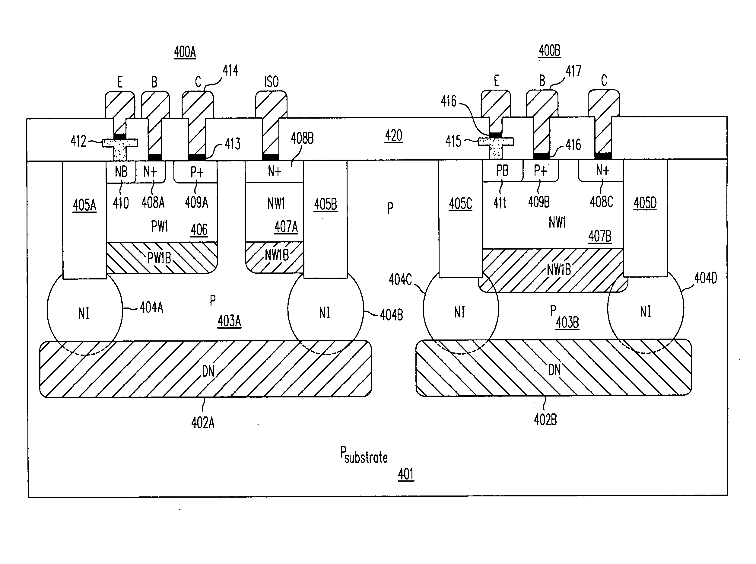
[0053]To eliminate the aforementioned limitations associated with prior art processes, the devices described herein are isolated using shallow, medium, or deep trench isolated regions (so called STI or DTI) instead of LOCOS. These dielectric-filled trenches are combined with high-energy and chained ion implantations to form floor isolation and to enhance sidewall isolation voltage capability.
[0054]The novel combination of STI or DTI for sidewall isolation and high energy implanted floor isolation represent in various forms, both method and apparatus inventive matter for integrating and isolating devices at high densities, without the need for long high-temperature diffusion or expensive epitaxial deposition. The isolation structures produced in this manner can be divided into three categories or “types”, which are herein defined as follows:[0055]Type-I isolation: a combination of deep high-energy ion implanted floor isolation and a dielectric-filled trench sidewall isolation, with t...
PUM
 Abstract
Description
Claims
Application Information