Method of producing group iii-v compound semiconductor, schottky barrier diode, light emitting diode, laser diode, and methods of fabricating the diodes

a technology of compound semiconductors and laser diodes, which is applied in the direction of semiconductor lasers, coatings, lasers, etc., can solve the problems of difficult control of n-type carrier density within a low density range, and achieve the effect of reducing n-type carrier density

Inactive Publication Date: 2008-10-16
SUMITOMO ELECTRIC IND LTD
View PDF7 Cites 18 Cited by
  • Summary
  • Abstract
  • Description
  • Claims
  • Application Information

AI Technical Summary

Benefits of technology

[0008]The present invention therefore contemplates a method of producing a group III-V compound semiconductor, a Schottky barrier diode, a light emitting diode, a laser diode, and a method of fabricating them, that can achieve a reduced n type carrier density.

Problems solved by technology

Conventionally it has been difficult to control n type carrier density within a low density range.

Method used


Image

  • Method of producing group iii-v compound semiconductor, schottky barrier diode, light emitting diode, laser diode, and methods of fabricating the diodes
  • Method of producing group iii-v compound semiconductor, schottky barrier diode, light emitting diode, laser diode, and methods of fabricating the diodes
  • Method of producing group iii-v compound semiconductor, schottky barrier diode, light emitting diode, laser diode, and methods of fabricating the diodes

Examples


first embodiment

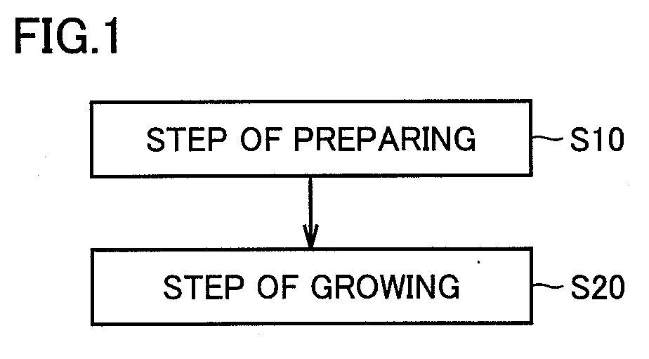
[0051]FIG. 1 is a flowchart of a method of producing a group III-V compound semiconductor in a first embodiment of the present invention. With reference to FIG. 1, the present invention in the first embodiment provides the method of producing a group III-V compound semiconductor, as will be described hereinafter. This method employs MOCVD with a group III element-containing material to produce a group III-V compound semiconductor.

[0052]In the method, as shown in FIG. 1, initially the step of preparing a seed substrate (S10) is performed. In the step of preparing (S10), for example, the seed substrate is mounted on a surface of a mount of a susceptor in an MOCVD apparatus and held by the susceptor.

[0053]While the seed substrate prepared in the step of preparing (S10) is not limited to a particular substrate, n type gallium nitride (GaN) can for example be used. Note that the seed substrate is formed preferably of the same material as the group III-V compound semiconductor grown in th...

second embodiment

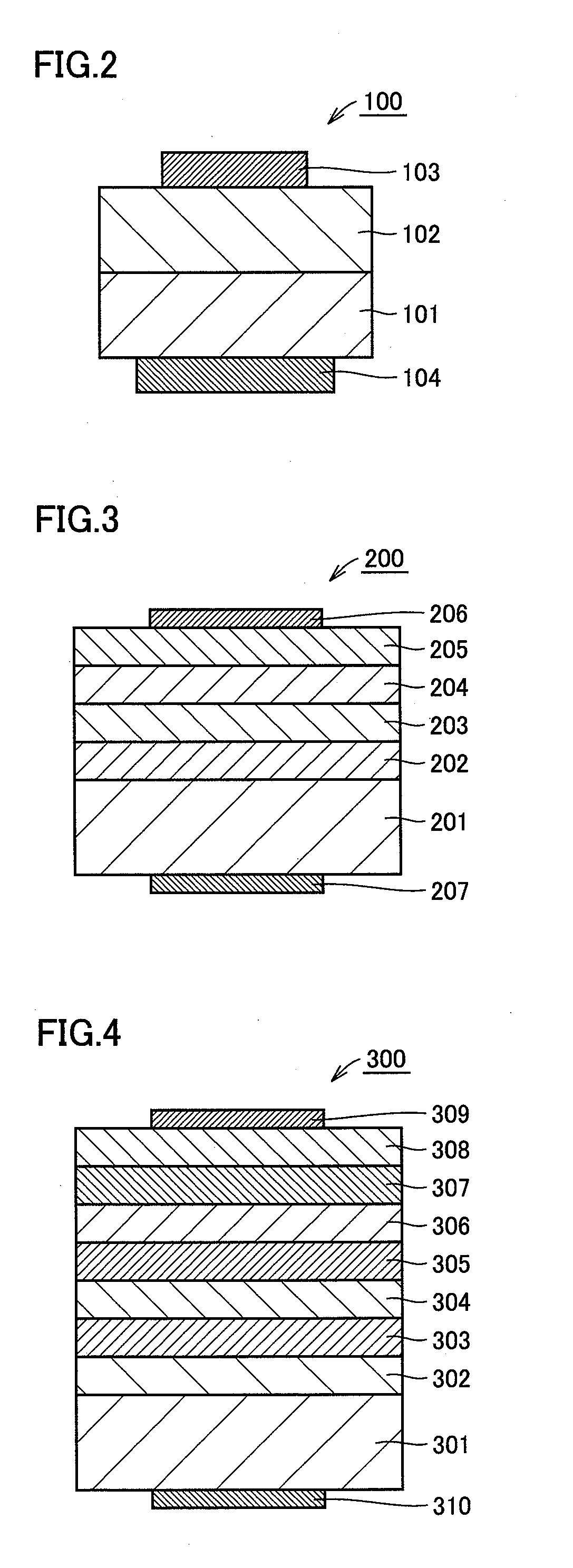
[0068]FIG. 2 is a schematic cross section of a Schottky barrier diode in a second embodiment of the present invention. With reference to FIG. 2, the present invention in the second embodiment provides the Schottky barrier diode, as will be described hereinafter. As shown in FIG. 2, the second embodiment provides a Schottky barrier diode 100 including a substrate 101, a drift layer 102, an anode electrode 103, and a cathode electrode 104.

[0069]Substrate 101 is an n type gallium nitride (GaN) substrate. Drift layer 102 is a layer formed of n type GaN and deposited on substrate 101. Drift layer 102 has a carrier density preferably of at least 5×1015 cm−3 and at most 5×1016 cm−3, more preferably at least 5×1015 cm−3 and at most 2×1016 cm−3. A carrier density of at least 5×1015 cm−3 allows Schottky barrier diode 100 to maintain low on-resistance when forward voltage is applied. A carrier density of at most 5×1016 cm−3 allows Schottky barrier diode 100 to have an improved breakdown voltag...

third embodiment

[0077]FIG. 3 is a schematic cross section of a light emitting diode in a third embodiment of the present invention. With reference to FIG. 3, the present invention in the third embodiment provides the light emitting diode, as will be described hereinafter. The third embodiment provides a light emitting diode 200 including an n type GaN substrate, and a layer formed of p type AlxGayIn(1-x-y)N and deposited on the n type GaN substrate, wherein 0≦x≦1, 0≦y≦1, and x+y≦1.

[0078]More specifically, as shown in FIG. 3, light emitting diode 200 includes a substrate 201, an n type buffer layer 202, an active layer 203, a p type electron block layer 204, a p type contact layer 205, a p type electrode 206, and an n type electrode 207.

[0079]Substrate 201 is an n type GaN substrate. N type buffer layer 201 is deposited on substrate 201 and formed for example of n type GaN. Active layer 203 is deposited on n type buffer layer 202 and configured for example of a multiquantum well structure formed of ...


PUM

PropertyMeasurementUnit
n type carrier densityaaaaaaaaaa
carrier densityaaaaaaaaaa

Abstract

There are provided a method of producing a group III-V compound semiconductor, a Schottky barrier diode, a light emitting diode, a laser diode and methods of fabricating the diodes, that can achieve a reduced n type carrier density. The method of producing a group III-V compound semiconductor is a method of producing the compound semiconductor by metal organic chemical vapor deposition employing a material containing a group III element. Initially the step of preparing a seed substrate is performed. Then the step of growing a group III-V compound semiconductor on the seed substrate is performed by employing as a group III element-containing material an organic metal containing at most 0.01 ppm of silicon, at most 10 ppm of oxygen and less than 0.04 ppm of germanium.

Description

BACKGROUND OF THE INVENTION[0001]1. Field of the Invention[0002]The present invention relates generally to methods of producing group III-V compound semiconductors, Schottky barrier diodes, light emitting diodes, laser diodes and methods of fabricating such diodes. For example the present invention relates to methods of producing group III-V compound semiconductors, Schottky barrier diodes, light emitting diodes, laser diodes and methods of fabricating such diodes, that can achieve a reduced n type carrier density.[0003]2. Description of the Background Art[0004]Group III-V compound semiconductor is significantly useful for Schottky barrier diodes, light emitting diodes (LEDs), laser diodes (LD) and other similar semiconductor devices. To produce such group III-V compound semiconductor, for example sublimination, hydride vapor phase epitaxy (HVPE), molecular beam epitaxy (MBE), metal organic chemical vapor deposition (MOCVD) and the like vapor phase epitaxy have conventionally been p...

Claims


Application Information

Patent Timeline
Patent Type & Authority Applications(United States)
IPC IPC(8): H01L21/20H01L29/47H01L33/00H01S3/042H01L33/06H01L33/32H01L33/36
CPCH01S5/2009B82Y20/00H01S5/3054H01S5/3211H01S5/34333H01S2304/04C23C16/303H01L21/02389H01L21/02458H01L21/02505H01L21/0254H01L21/0257H01L21/02576H01L21/0262H01L29/872H01L33/0075H01L33/325H01L29/66212H01L29/66462H01L29/7786H01L29/2003H01S5/305
Inventor UENO, MASAKISAITOH, YU
Owner SUMITOMO ELECTRIC IND LTD
Why Eureka
Try Eureka