Memory device and semiconductor device

a memory device and semiconductor technology, applied in static storage, digital storage, instruments, etc., can solve the problems of data writing, insufficient amount of charge, damage or deformation of memory elements, etc., and achieve the effect of reducing the number of transistors in one memory cell, suppressing power consumption in data writing, and reducing the siz

Active Publication Date: 2011-09-22
SEMICON ENERGY LAB CO LTD
View PDF99 Cites 8 Cited by
  • Summary
  • Abstract
  • Description
  • Claims
  • Application Information

AI Technical Summary

Benefits of technology

[0021]In a second memory portion, a transistor with the aforementioned structure is used as a switching element for controlling holding of charge in a memory element, whereby charge can be prevented from leaking from the memory element. Therefore, the second memory portion with the aforementioned structure can hold data for a longer period of time as compared to the case of using a DRAM. Thus, refresh operation is not needed in the verifying operation. Further, it is not necessary to supply voltage to the second memory portion with the aforementioned structure all the time when data is held, which is different from the case of using

Problems solved by technology

In a flash memory or an EEPROM, a defect in data writing is caused by the following problems, for example: a sufficient amount of charge is not accumulated in a floating gate because voltage applied to a memory element is too low; and a memory element is damaged or degraded because volta

Method used


Image

  • Memory device and semiconductor device
  • Memory device and semiconductor device
  • Memory device and semiconductor device

Examples


embodiment 1

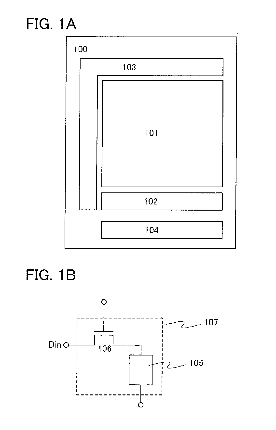
[0041]FIG. 1A illustrates a block diagram of a structure of a memory device according to one embodiment of the present invention, as an example. A memory device 100 illustrated in FIG. 1A includes a first memory portion 101, a second memory portion 102, a driver circuit 103, and a comparison circuit 104.

[0042]A plurality of memory cells each including a nonvolatile memory element are provided in the first memory portion 101. Further, a plurality of memory cells each including a memory element and a transistor are provided in the second memory portion 102. The transistor is provided to control the holding of charge in the memory element; the off-state current or the leakage current of the transistor is extremely low.

[0043]The driver circuit 103 controls the operation of the first memory portion 101. Specifically, various kinds of operation such as the writing of data into the first memory portion 101, the reading of data from the first memory portion 101, the holding of data in the f...

embodiment 2

[0111]The operation of the memory device of one embodiment of the present invention is described in more detail.

[0112]In this embodiment, the case where 8-bit data is written into a specified memory region including a plurality of memory cells is given as an example and the operation of the first memory portion is described. FIG. 4 schematically illustrates the flow of data written into the second memory portion in the operation of writing data into the first memory portion, as an example. In FIG. 4, four memory regions included in the second memory portion are used as four data buffers.

[0113]A memory region included in each data buffer has a memory capacity in which data having the same number of bits as data written into the first memory portion can be stored. In this embodiment, each data buffer includes at least a memory region for storing 8-bit data.

[0114]A data buffer for reference data which is shown in FIG. 4 is a data buffer for temporarily storing data (reference data) tra...

embodiment 3

[0144]In this embodiment, a structure of the second memory portion and the operation thereof are described.

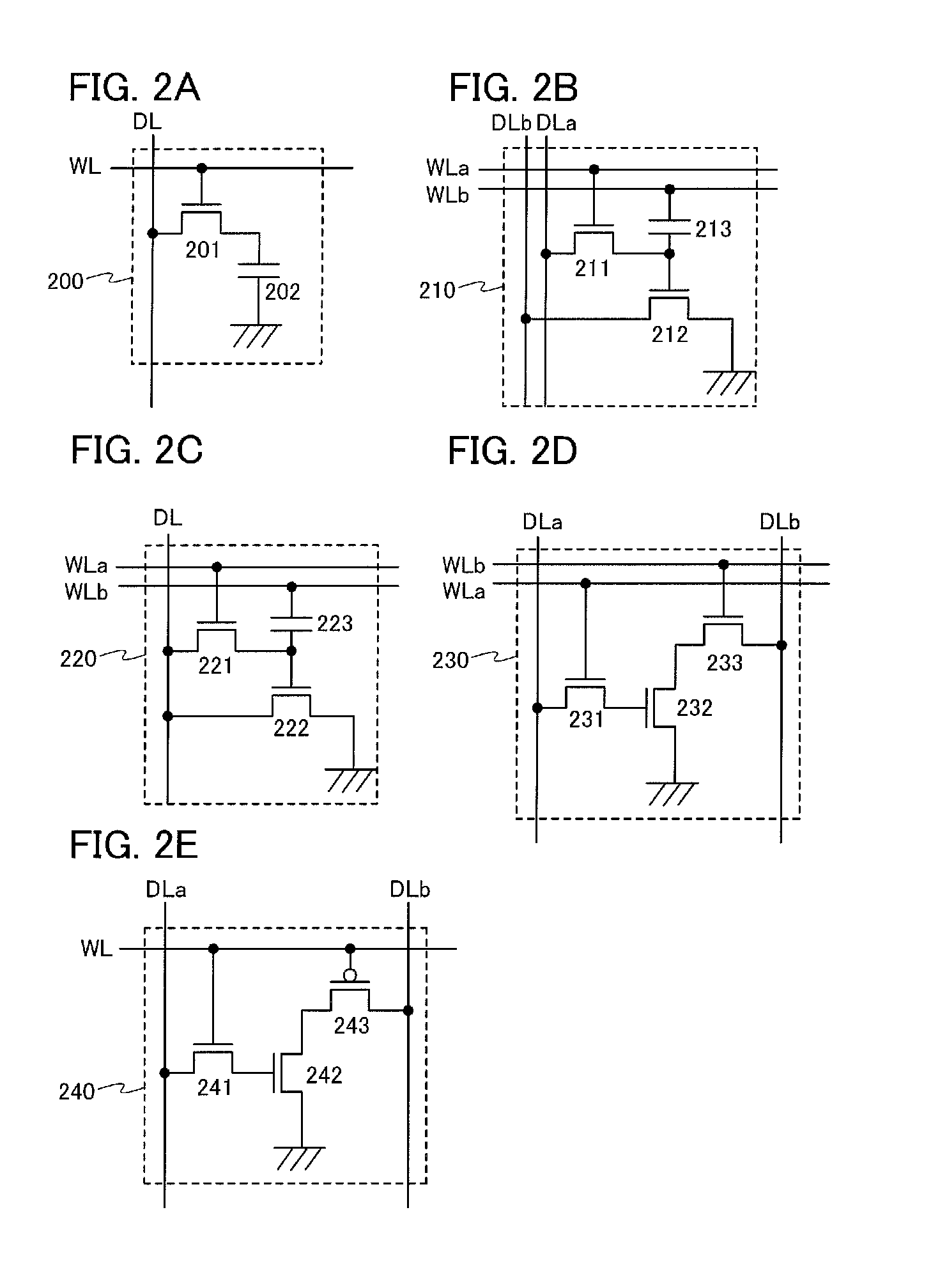
[0145]FIG. 6 illustrates an example of the circuit diagram of a second memory portion 205 including a plurality of memory cells 200 one of which is shown in FIG. 2A. For the structure of the memory cell 200, the description in Embodiment 1 can be referred to.

[0146]In the second memory portion 205 shown in FIG. 6, a variety of wirings such as a plurality of word lines WL and a plurality of data lines DL are provided, and a signal or a fixed potential from a driver circuit of the second memory portion 205 is supplied to each memory cell 200 through the wirings. The number of the wirings can be determined by the number of the memory cells 200 and arrangement of the memory cells 200.

[0147]Specifically, the second memory portion 205 shown in FIG. 6 is an example in which memory cells are connected in a matrix with three rows and four columns and word lines WL1 to WL3 and data lines ...


PUM


Abstract

One of objects is to provide a nonvolatile memory device in which the occurrence of a defect in data writing is suppressed and whose area can be suppressed, or a semiconductor device including the nonvolatile memory device. A first memory portion including a nonvolatile memory element and a second memory portion (data buffer) for temporarily storing data in verifying operation in which whether the data is correctly written into the first memory portion is verified are provided. Further, the second memory portion includes a memory element and an insulated gate field effect transistor for controlling the holding of charge in the memory element; the off-state current or the leakage current of the transistor is extremely low.

Description

TECHNICAL FIELD[0001]The present invention relates to a nonvolatile memory device and a semiconductor device including the memory device.BACKGROUND ART[0002]A nonvolatile semiconductor memory device (hereinafter, simply referred to as a memory device) which is capable of writing and erasing data repeatedly, such as an EEPROM or a flash memory, is convenient and has high resistance to physical impact. Therefore, it has been mainly used for a portable memory medium such as a USB flash drive or a memory card, an RF tag which is a medium for radio frequency identification (RFID) in which data is read wirelessly, or the like, and has been widely available on the market. In the memory device, a transistor which functions as a memory element is included in each memory cell. Further, the transistor has an electrode called a floating gate, between a gate electrode and a semiconductor film serving as an active layer. The accumulation of charge in the floating gate enables storage of data.[000...

Claims


Application Information

Patent Timeline
IPC IPC(8): G11C14/00G11C16/04
CPCG11C11/404G11C11/405G11C16/26G11C16/0433G11C14/00
Inventor SAITO, TOSHIHIKONAGATSUKA, SHUHEI
Owner SEMICON ENERGY LAB CO LTD
Why Eureka
Try Eureka