Display device, method for manufacturing display device, and SOI substrate
a display device and substrate technology, applied in the direction of semiconductor devices, basic electric elements, electrical apparatus, etc., can solve the problems of low bonding strength of the soi layer, inability to heat treatment at a high temperature, and difficulty in forming a soi layer over the substrate, etc., to achieve improved production efficiency and high performance , the effect of improving the productivity of manufacturing display devices
- Summary
- Abstract
- Description
- Claims
- Application Information
AI Technical Summary
Benefits of technology
Problems solved by technology
Method used
Image

Examples
embodiment modes
[0045]Hereinafter, embodiment modes of the present invention are described in detail with reference to the drawings. Note that the present invention is not limited to the following description, and it is easily understood by those skilled in the art that the modes and details disclosed herein can be modified in various ways without departing from the spirit and scope of the present invention. Therefore, the present invention should not be interpreted as being limited to the description of the embodiment modes to be given below. In the structures of the present invention to be described hereinafter, a reference numeral which designates the same parts is used in different drawings in some cases.
embodiment mode 1
[0046]An SOI substrate according to this embodiment mode is formed by transferring single-crystalline semiconductor layers from a single-crystalline semiconductor substrate to a substrate of a different type (hereinafter, also referred to as a “base substrate”). Hereinafter, an SOI substrate according to this embodiment mode and an embodiment mode of a method for manufacturing the SOI substrate are described.
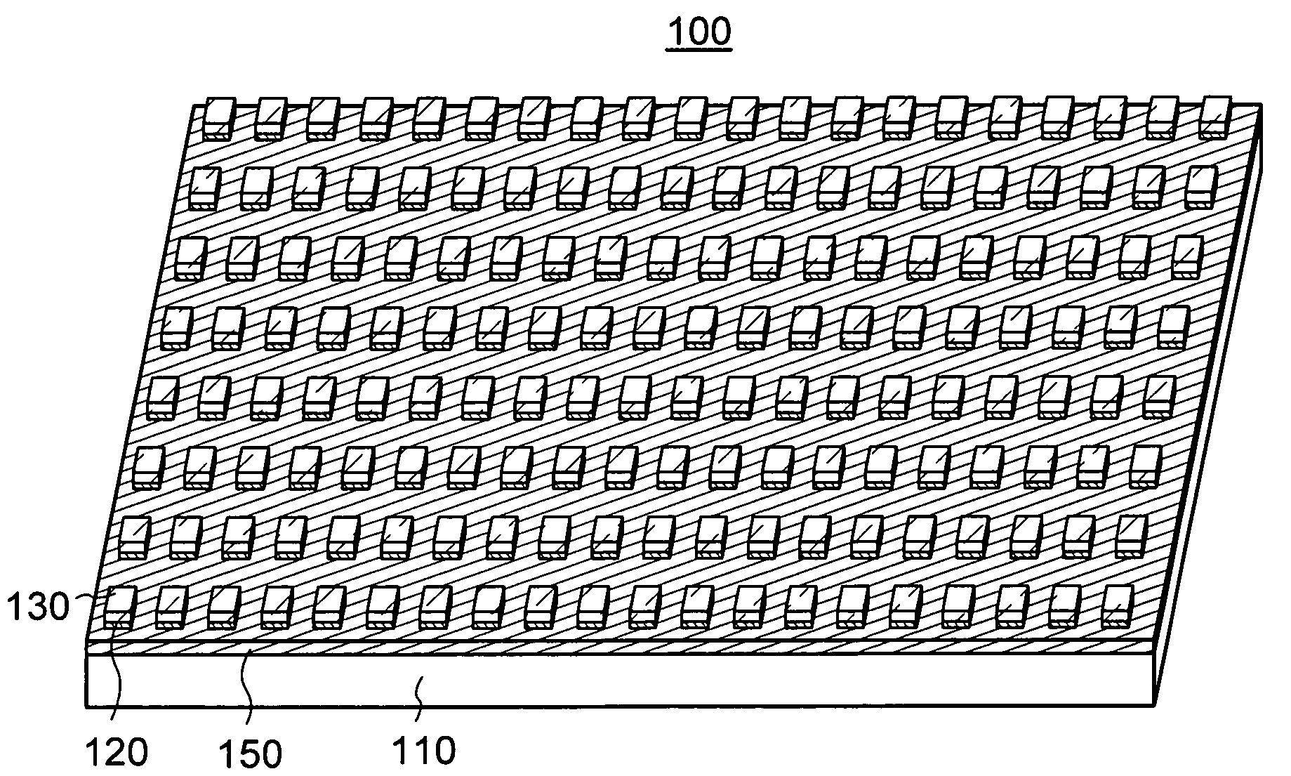
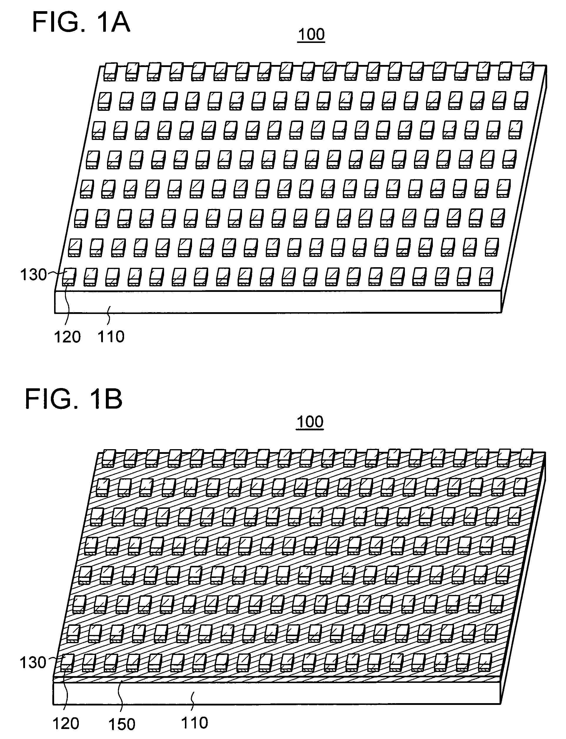
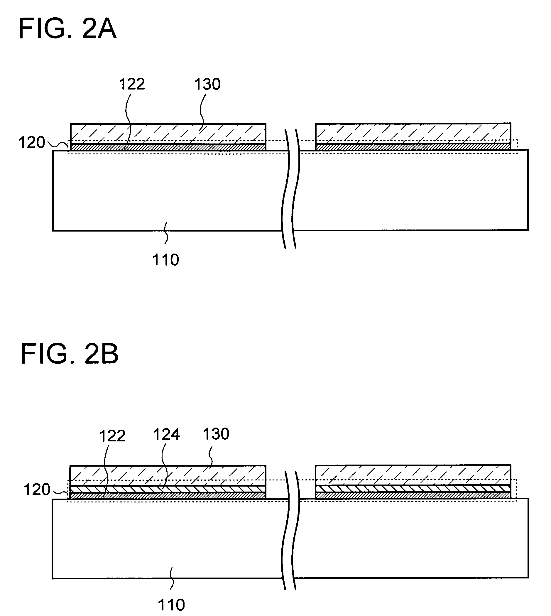
[0047]FIGS. 1A and 1B show perspective views showing structural examples of an SOI substrate according to the present invention. Further, FIGS. 2A to 3B show cross-sectional views of examples of an SOI substrate according to the present invention.
[0048]In FIGS. 1A, 2A, and 2B, an SOI substrate 100 has a structure in which a plurality of layered bodies in which an insulating layer 120 and a single-crystalline semiconductor layer (hereinafter, also referred to as an SOI layer) 130 are stacked in this order are provided over a surface of a base substrate 110. The SOI layer 130 is p...
embodiment mode 2
[0176]This embodiment mode shows an example in which an SOI substrate is manufactured by a different method from the above embodiment mode.
[0177]First, a semiconductor substrate 200 is provided (see FIG. 23A). For the semiconductor substrate 200, a substrate similar to the semiconductor substrate 101 may be used: for example, a silicon substrate, a germanium substrate, or a compound semiconductor substrate of gallium arsenide, indium phosphide, or the like may be used.
[0178]It is preferable that an insulating layer 202 containing nitrogen be formed over one surface of the semiconductor substrate 200. The insulating layer 202 containing nitrogen may be formed using a silicon nitride layer, a silicon nitride oxide layer, or a silicon oxynitride layer to have a single-layer structure or a stacked-layer structure. Provision of the insulating layer 202 containing nitrogen can prevent impurities such as movable ions or moisture from being diffused into an SOI layer and thus contaminating ...
PUM
 Abstract
Description
Claims
Application Information
 - R&D
- Intellectual Property
- Life Sciences
- Materials
- Tech Scout
- Unparalleled Data Quality
- Higher Quality Content
- 60% Fewer Hallucinations
Browse by: Latest US Patents, China's latest patents, Technical Efficacy Thesaurus, Application Domain, Technology Topic, Popular Technical Reports.
© 2025 PatSnap. All rights reserved.Legal|Privacy policy|Modern Slavery Act Transparency Statement|Sitemap|About US| Contact US: help@patsnap.com