
Electrostatic chuck

a technology of electrostatic chuck and chuck body, which is applied in the direction of electrostatic holding device, basic electric elements, electric apparatus, etc., can solve the problems of increasing the manufacturing cost of electrostatic chuck, poor adhesion to wafer, and insufficient heat dissipation, etc., to achieve low level of particulate generation, improve cooling performance and insulation performance, and facilitate ion implantation. the effect of smooth operation

Inactive Publication Date: 2008-10-30
SHIN ETSU CHEM IND CO LTD
View PDF14 Cites 29 Cited by
  • Summary
  • Abstract
  • Description
  • Claims
  • Application Information

AI Technical Summary

Benefits of technology

[0010]It is therefore an object of the present invention to provide an electrostatic chuck having superior cooling performance, insulating performance and a low level of particulate generation compared to those of the prior art.
[0014]Since the electrostatic chuck of the present invention has superior cooling performance and insulation performance and also has a low level of particulate generation, it is suitable for processes wherein a substrate must be held during manufacture of a semiconductor integrated circuit. In particular, when used in an ion implantation process, the temperature of a wafer can be kept uniform and constant, and ion implantation can be performed smoothly without causing heat damage to the wafer.

Problems solved by technology

However, since the ceramic insulating layer has a high hardness, it has poor adhesion to a wafer with surface unevenness, and since the contact thermal resistance increases as a result, sufficient heat dissipation is not obtained.
However, in this method, not only is it necessary to perform fine machining to form a groove in the insulating layer surface through which the inert gas can be passed, but an apparatus is required to supply the inert gas, and since the structure of the electrostatic chuck becomes more complex, there is a disadvantage of increasing the manufacturing cost of the electrostatic chuck.
Moreover, since the insulating layer is hard and particles are generated when the wafer is brought into contact and rubs against it, if the wafer is processed with particles still adhering to its back side, defects may occur during the fine machining of the wafer.
Although an electrostatic chuck using an insulating layer made from polyimide can be manufactured easily and is also economical, there is a problem that since it has a low thermal conductivity and is hard, it has a large contact thermal resistance, and heat dissipation properties are poor.
Also, as in the case of an electrostatic chuck using a ceramic insulating layer, there is the problem that particles are generated.
Moreover, since silicone rubber is soft, even if it comes in contact with a wafer, it does not easily generate particles, and a low level of particulate generation can be realized.
However, in recent years, still higher heat dissipation properties and lower particulate levels are being demanded, and in this respect, the performance of this electrostatic chuck is inadequate.
However, in the case of this electrostatic chuck, since sputter metal is introduced, there is concern about insulation abnormalities arising in the second insulating layer.
Further, in this electrostatic chuck, there is also concern that thermally conductive fillers such as alumina and boron nitride which are added to impart thermal conductivity to the silicone rubber may drop out, and generate the undesirable particles mentioned hereinabove.
However, if the specific surface area of a thermally conductive filler added to the silicone rubber of the third insulating layer is small, there is concern that it will be only weakly integrated with the silicone polymer, and since it has no active sites, which can bind to the silicone polymer, on the surface, particles may be generated.
Moreover, the thermally conductive filler is hard and may abrase the wafer by rubbing, which may also generate more particles.

Method used


Image

  • Electrostatic chuck
  • Electrostatic chuck
  • Electrostatic chuck

Examples


example 1

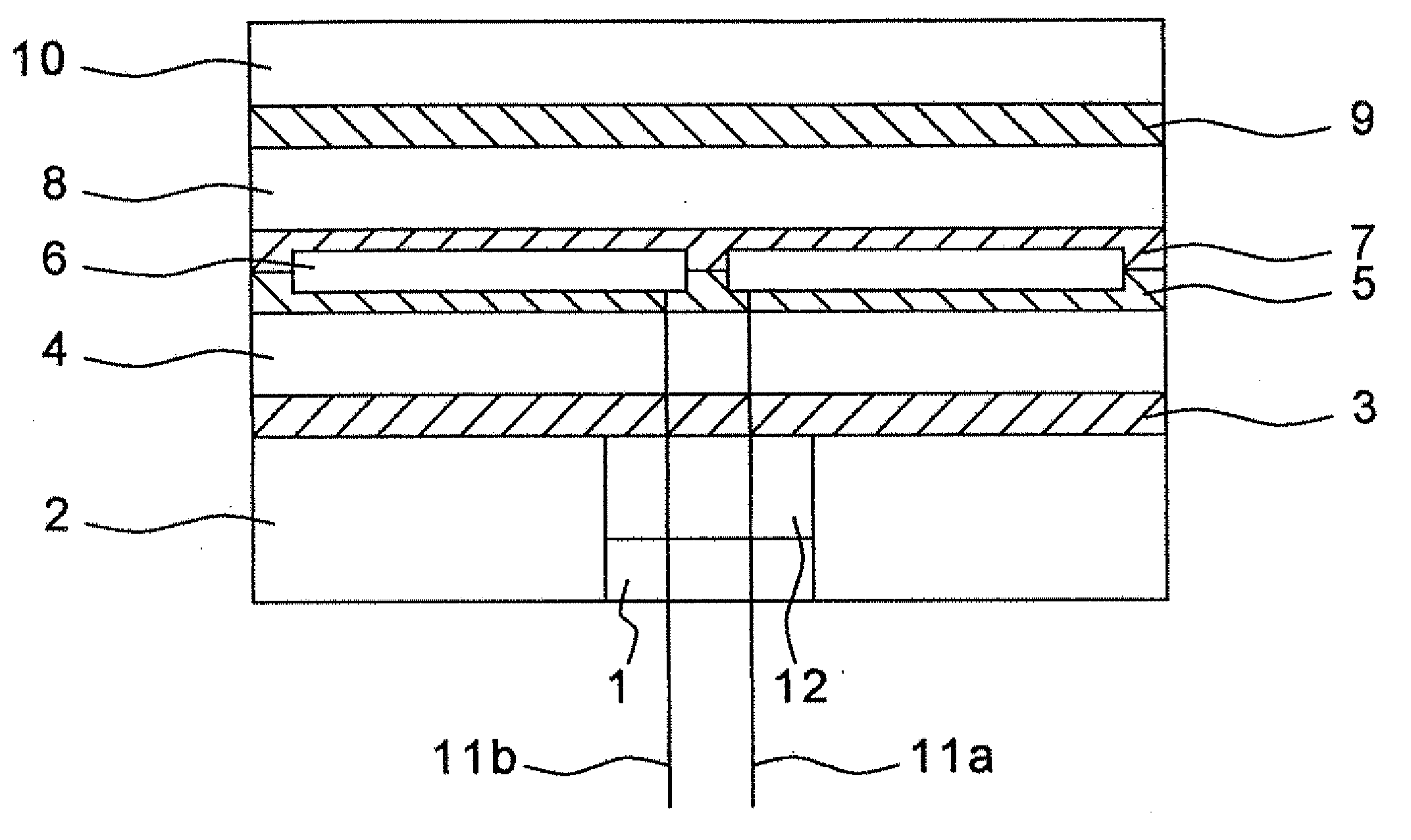
[0055]The electrostatic chuck having the structure shown in FIG. 1 was produced as follows.

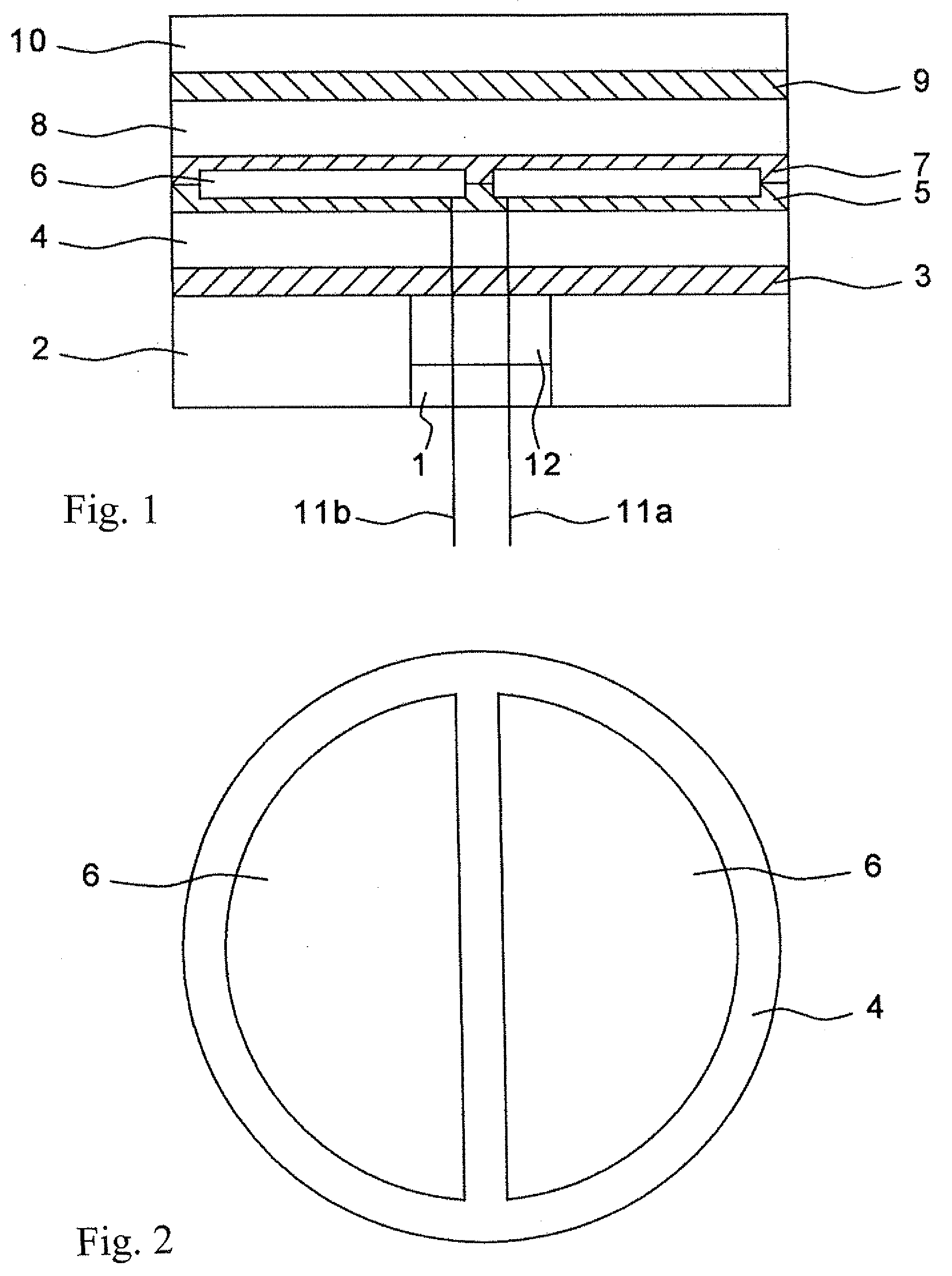
[0056]Primer No. 24T (product name, Shin-Etsu Chemical Co., Ltd.) as an adhesive was applied to one side of an electrolytic copper foil (thickness 35 μm) using a brush, and was air-dried for 30 minutes at room temperature to obtain the adhesive layer 5 (thickness 10 μm). The adhesive layer 5 and the first insulating layer 4 comprising an unvulcanized sheet of thermally conductive silicone rubber TC-65BG (product name, Shin-Etsu Chemical Co., Ltd. thickness 650 μm, thermal conductivity 4 W / mK) containing boron nitride were stuck together, and press bonding was performed for 10 minutes at a pressure of 5 MPa and temperature of 170□. Chemical etching of the electrolytic copper foil was performed, and the electrically conducting pattern 6 (copper electrode) having the shape shown in FIG. 2 was thus formed on the first insulating layer 4.

[0057]Next, the liquid silicone rubber adhesive KE1825 (produ...

example 2

[0061]Next, an electrostatic chuck was produced as in Example 1, except the conditions were changed as follows.

(1) Instead of the third insulating layer 10 comprising an unvulcanized sheet of silicone rubber A, the third insulating layer 10 of an unvulcanized sheet of a silicone rubber B (thickness 120 μm, the properties of cured silicone rubber A were: hardness 63, tensile strength 8.8 MPa and surface roughness 0.5 μm), which was prepared by blending 100 mass parts of an organo-polysiloxane (composition, methylvinylpolysiloxane having an average degree of polymerization of 8000 comprising 99.85 mol % of dimethylsiloxane units and 0.15 mol % of methylvinyl siloxane units) with 50 mass parts of fumed silica Aerosil 200 (product name, Japan Aerosil Co., Ltd.) having a specific surface area of 200 m2 / g, and 0.7 mass parts of 2,5-dimethyl-2,5-di(tert-butylperoxy) hexane, was used.

(2) Instead of the second insulating layer 8 comprising a 25 μm-thick polyimide film, the second insulating ...

example 3

[0062]An electrostatic chuck was produced as in Example 1, except that instead of the liquid silicone rubber adhesive KE1825 used for the adhesive layer 7 and adhesive layer 3, a thermally conductive silicone rubber adhesive KE1862 (product name, Shin-Etsu Chemical Co., Ltd.) was used.

Evaluation of Electrostatic Chucks of Examples 1-3

Cooling Performance

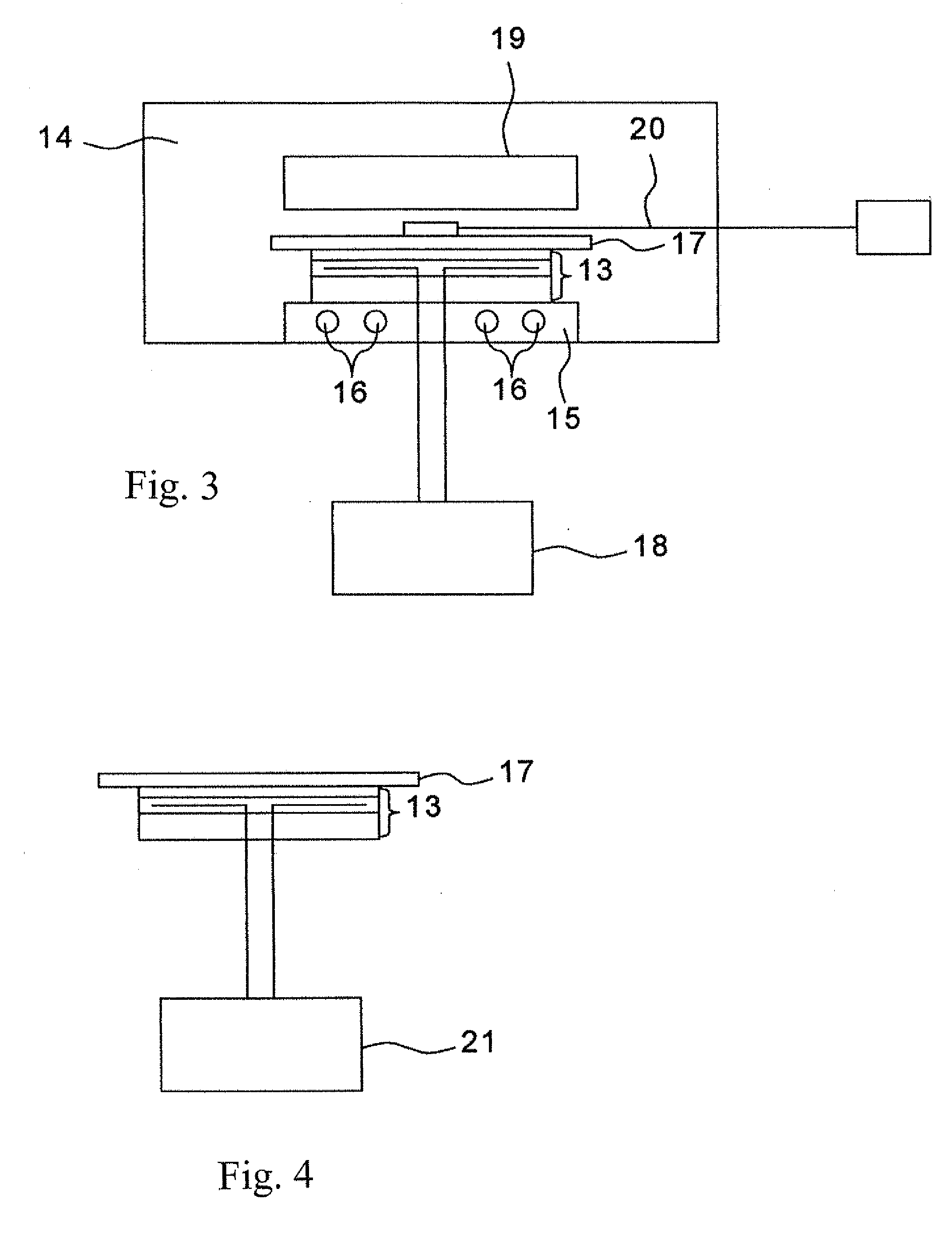
[0063]The cooling performance of each of the electrostatic chucks obtained in Examples 1-3 was evaluated. A cooling performance tester was used for the evaluation. FIG. 3 is a longitudinal cross-section showing an outline of the construction of the cooling performance tester. In FIG. 3, 13 is an electrostatic chuck, 14 is a chamber, 15 is a stand, 16 are cooling tubes, 17 is a wafer, and 18 is a power supply. The electrostatic chuck 13 is mounted on the stand 15 in the chamber 14, and cooling water is circulated through the cooling tube provided on the stand 15 to cool the electrostatic chuck 13. After installing the wafer 17 on the e...


PUM


Abstract

This invention relates to a suitable electrostatic chuck to hold a substrate during the manufacture of a semiconductor integrated circuit having excellent cooling performance and insulation performance, and a low level of particulate generation, which is comprised of an electrostatic chuck, comprising a metal substrate, a first insulating layer of silicone rubber formed directly or via an adhesive layer on the metal substrate and having a thermal conductivity of 0.5 W / mK or more, an electrically conducting pattern formed directly or via an adhesive layer on this first insulating layer, a second insulating layer of an insulating polyimide film formed directly or via an adhesive layer on this electrically conducting pattern, and a third insulating layer formed directly or via an adhesive layer on this second insulating layer, wherein this third insulating layer is a silicone rubber containing reinforcing silica, this layer not containing any thermally conductive filler having an average particle size of 0.5 μm or more.

Description

FIELD OF THE INVENTION[0001]The present invention relates to an electrostatic chuck used in a process for holding a substrate required in the manufacture of a semiconductor integrated circuit, and in particular, to an electrostatic chuck useful in an ion implantation process, a sputtering process, a plasma etching process, and the like.BACKGROUND OF THE RELATED ART[0002]In the prior art, an electrostatic chuck known as an electrostatic adsorption wafer chuck is used to hold a substrate during the manufacture of a semiconductor integrated circuit. As an insulating layer of this electrostatic chuck, alumina, aluminum nitride, a ceramic material such as boron nitride, an organic resin such as a polyimide, or a elastic body such as silicone rubber, has been proposed.[0003]In an ion implantation process, it is required to perform ion implantation smoothly wherein the temperature rise of a wafer due to the heat of an ion beam is suppressed, the temperature of the wafer is kept uniform and...

Claims


Application Information

Patent Timeline
Patent Type & Authority Applications(United States)
IPC IPC(8): H01T23/00
CPCH01L21/6831H02N13/00
Inventor HANDA, RYUICHINAKANO, AKIOSAKURAI, IKUO
Owner SHIN ETSU CHEM IND CO LTD
Features
  • Generate Ideas
  • Intellectual Property
  • Life Sciences
  • Materials
  • Tech Scout
  • Unparalleled Data Quality
  • Higher Quality Content
  • 60% Fewer Hallucinations
Learn More