
Method of making high efficiency UV vled on metal substrate

a technology of light-emitting diodes and metal substrates, applied in semiconductor/solid-state device manufacturing, electrical equipment, semiconductor devices, etc., can solve the problems of limiting the thickness of semiconductor layers in the led stack, significant or total efficiency loss, and slow layer growth rate of alingan and alingan, so as to achieve faster growth rate and increase crystalline quality

Active Publication Date: 2008-11-06
SEMILEDS OPTOELECTRONICS CO LTD
View PDF8 Cites 8 Cited by
  • Summary
  • Abstract
  • Description
  • Claims
  • Application Information

AI Technical Summary

Benefits of technology

[0008]Embodiments of the present invention generally provide techniques for fabricating vertical light-emitting diode (VLED) structures composed of AlInGaN or AlGaN with increased crystalline quality and a faster growth rate when compared to conventional AlInGaN or AlGaN LED structures.

Problems solved by technology

Therefore, a semiconductor layer of gallium nitride (GaN) is most likely not present outside the active layer(s) in the UV LED structure; otherwise, the emitted light would be absorbed by the GaN layer(s), resulting in a significant or total loss of efficiency.
However, the layer growth rate of AlGaN and AlInGaN is very slow, especially with high aluminum (Al) content, due to trimethylaluminum (Al(CH3)3)-ammonia (TMA-NH3) adduct formation.
In addition, a thick AlGaN or AlInGaN layer will often crack, thereby limiting the thickness of the semiconductor layers in the LED stack.
For example, an AlGaN layer directly grown on sapphire with 20% Al and a thickness of 0.4 μm has been observed to develop very poor morphology with microcracking along certain preferential crystallographic directions.
Moreover, the dislocation density for AlInGaN or AlGaN layers grown directly on a sapphire substrate may be unacceptable for a desired level of performance from a UV LED.
These lattice imperfections, or dislocations, may have a profound limiting effect on light emission efficiency from the LED.

Method used


Image

  • Method of making high efficiency UV vled on metal substrate
  • Method of making high efficiency UV vled on metal substrate
  • Method of making high efficiency UV vled on metal substrate

Examples


Embodiment Construction

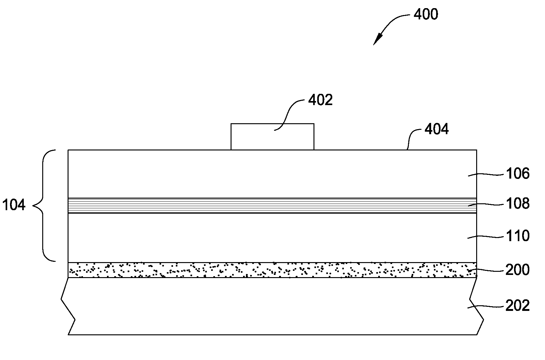
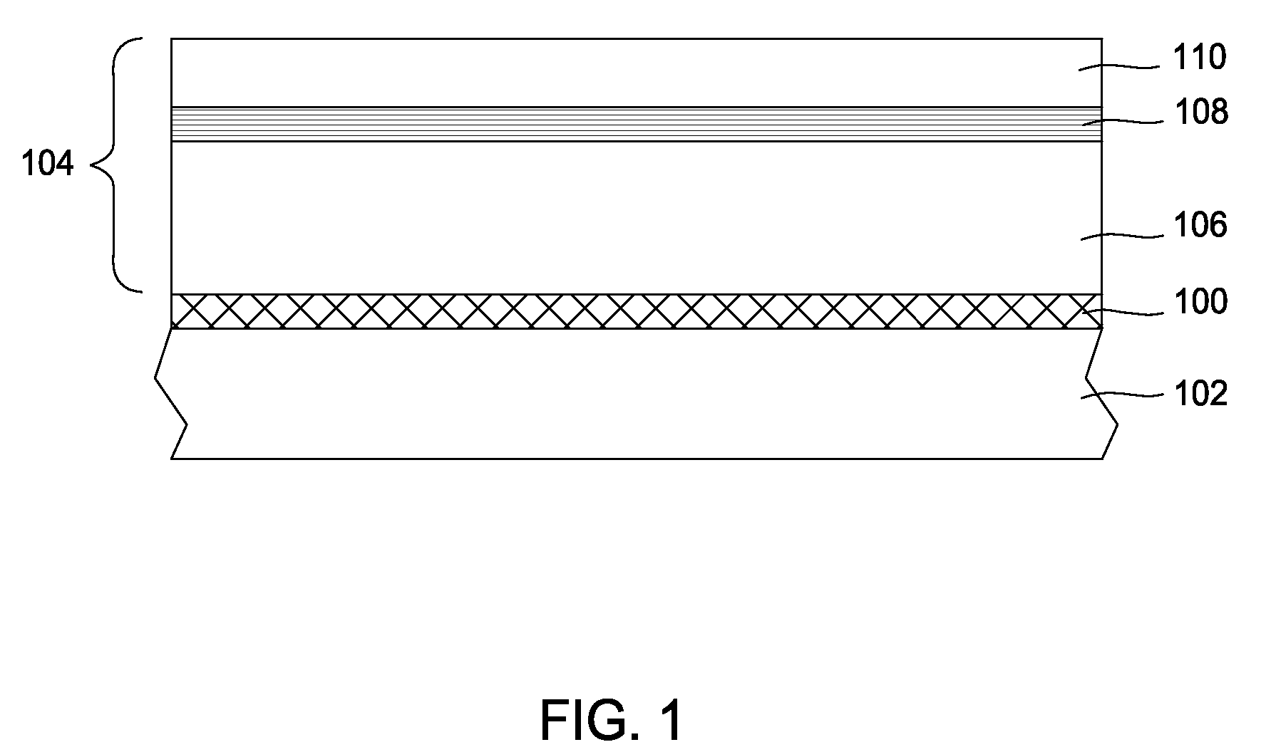
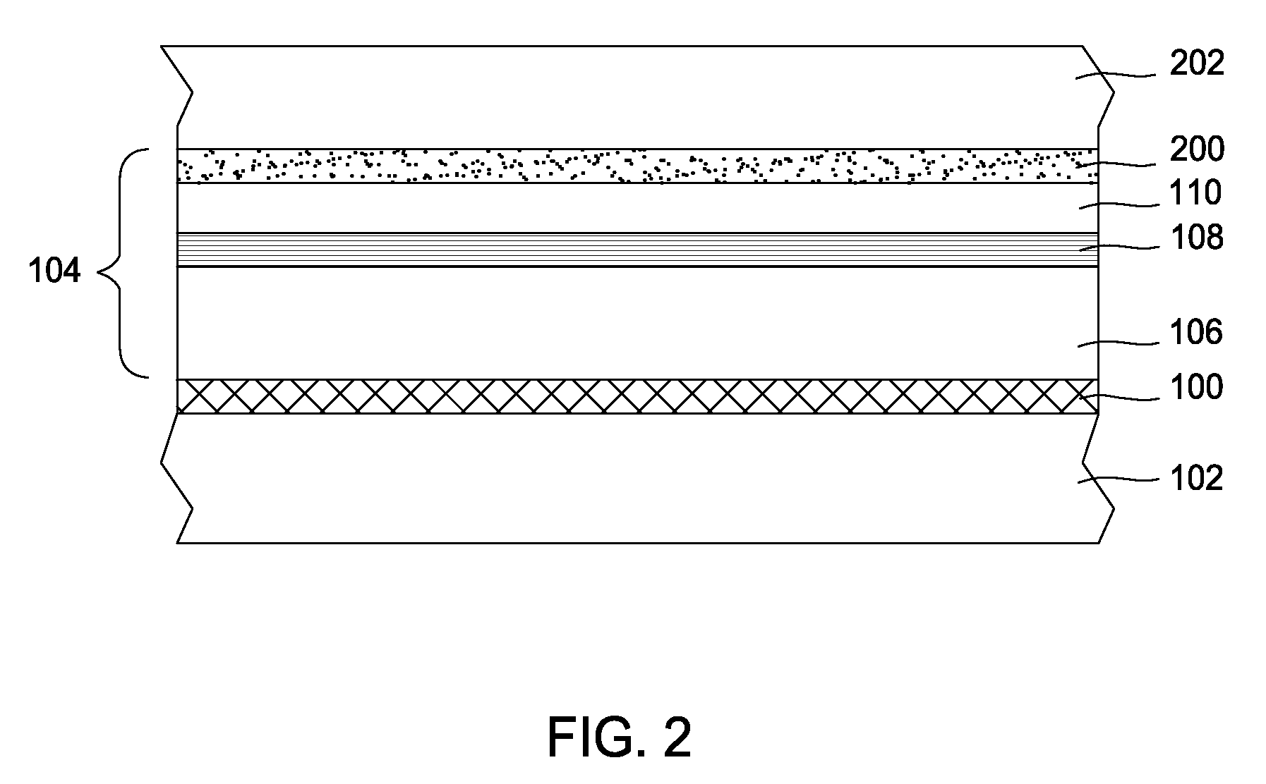
[0016]Embodiments of the present invention generally provide techniques for fabricating ultraviolet (UV) vertical light-emitting diode (VLED) structures composed of AlInGaN or AlGaN with increased crystalline quality and a faster growth rate when compared to conventional AlInGaN or AlGaN LED structures. This may be accomplished by forming a sacrificial GaN layer above a carrier substrate, and then depositing the light-emitting diode (LED) stack above the sacrificial GaN layer.

An Exemplary VLED Fabrication Method

[0017]Referring now to FIG. 1, a sacrificial GaN layer 100 may be deposited on a carrier substrate 102 employing various techniques known to those skilled in the art, such as metalorganic chemical vapor deposition (MOCVD), molecular beam epitaxy (MBE), and hydride vapor phase epitaxy (HVPE). Being an n-doped, p-doped, or undoped layer, the thickness of the sacrificial GaN layer 100 may range from about 10 nm to 10 μm. A doped sacrificial GaN layer 100 may be doped with silico...


PUM

PropertyMeasurementUnit
thicknessaaaaaaaaaa
thicknessaaaaaaaaaa
thicknessaaaaaaaaaa

Abstract

A method of fabricating ultraviolet (UV) vertical light-emitting diode (VLED) structures composed of AlInGaN or AlGaN with increased crystalline quality and a faster growth rate when compared to conventional AlInGaN or AlGaN LED structures is provided. This may be accomplished by forming a sacrificial GaN layer above a carrier substrate, and then depositing the light-emitting diode (LED) stack above the sacrificial GaN layer. The sacrificial GaN layer may then be removed in subsequent processing steps.

Description

BACKGROUND OF THE INVENTION[0001]1. Field of the Invention[0002]Embodiments of the present invention generally relate to the field of light-emitting diode (LED) technology and, more particularly, to a vertical light-emitting diode (VLED) structure.[0003]2. Description of the Related Art[0004]LEDs have been around for several decades, and research and development efforts are constantly being directed towards improving their luminous efficiency, thereby increasing the number of possible applications. To fabricate LEDs emitting near to far ultraviolet (UV) light, semiconductor layers comprising aluminum gallium nitride (AlGaN) or aluminum indium gallium nitride (AlInGaN) are typically epitaxially grown directly on a sapphire substrate using metal organic chemical vapor deposition (MOCVD). Such UV LEDs generally have an emission wavelength shorter than the energy bandgap of GaN (approximately 365 nm at room temperature). Therefore, a semiconductor layer of gallium nitride (GaN) is most ...

Claims


Application Information

Patent Timeline
Patent Type & Authority Applications(United States)
IPC IPC(8): H01L33/00
CPCH01L33/0079H01L33/007H01L33/0093H01L21/20H01L33/20
Inventor TRAN, CHUONG ANH
Owner SEMILEDS OPTOELECTRONICS CO LTD
Learn More