Imaging Device by Buried Photodiode Structure
a photodiode and imaging device technology, applied in the field of pixel structure, can solve problems such as the generation of reset noise, and achieve the effects of low dark current, high sensitivity, and sufficient storage signal amoun
- Summary
- Abstract
- Description
- Claims
- Application Information
AI Technical Summary
Benefits of technology
Problems solved by technology
Method used
Image

Examples
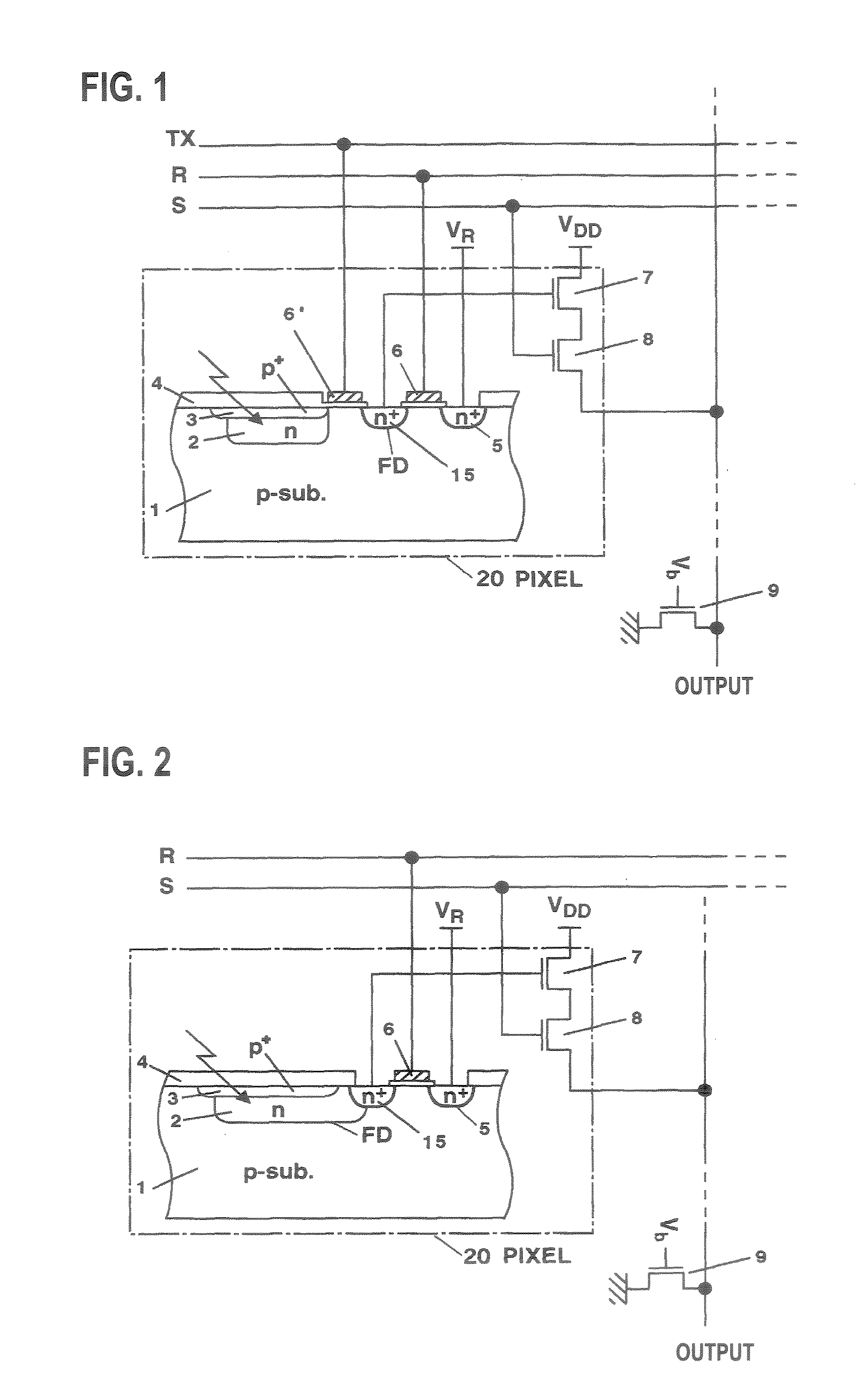
first embodiment
[0036]FIG. 3 shows an example of its structure, which is based on architecture that directly detects the potential of the photodiode without transferring a signal charge; inside the pixel. The n-type region serving as a charge storage region (2) of t he photodiode is buried in a substrate (1). The interface between a silicon and a silicon oxide film (4) is covered with a p-layer (3) of high concentration, and a p-layer (11) of a relatively low concentration is formed only in the portion immediately below a floating electrode (14) adapted for signal extraction. The electrons generated by light are stored in the n-type region serving as the charge storage region (2), and the potential of the portion of the p-layer (11) at the surface of the semiconductor region is changed thereby. The change in the potential is transmitted through a thin insulating film to the floating electrode (14) in a floating state by the capacitive coupling. The change in the potential of the floating electrode ...
second embodiment
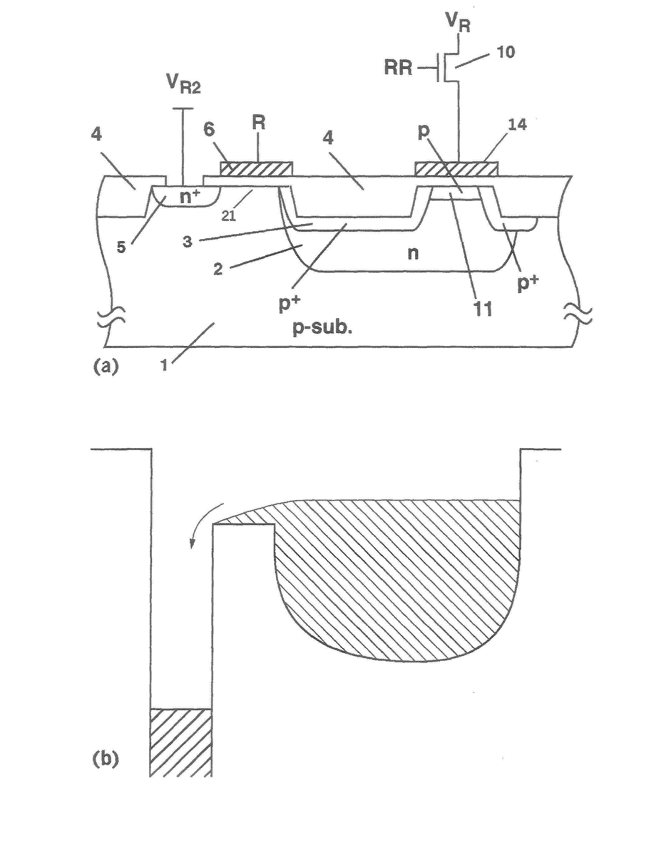
[0057]Instead of the above-explained floating electrode, architecture using a floating diffusion formed by doping impurities of the opposite polarity in the region disposed on the photodiode is explained. FIG. 9 shows its structure view. FIG. 9A is a top view, and FIG. 9B is a sectional view taken on line X-X. Let us suppose that the p-type substrate (1) is connected to 0 V. A first transfer transistor (21) encompasses a gate electrode provided above an interface between a charge storage region (2) and an n+ region (5). A second transfer transistor (10) encompasses a gate electrode (6) provided above a p-layer (22) of low concentration. Although the p+ region, to which the potential VR is applied, is illustrated as if the p+ region surrounds the periphery of the gate electrode (6), there is an empty space where the p+ region is not arranged on a part, which is ascribable to a manufacturing process.
[0058]FIG. 10 shows the readout operation timing. When 0 V or negative voltage is appl...
third embodiment
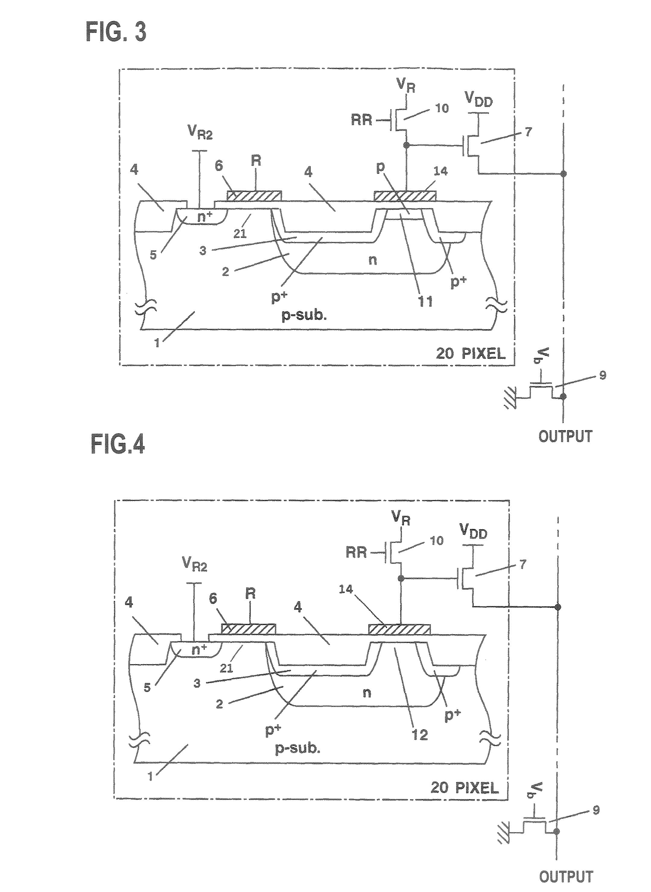
[0064]In the pixel device of the present invention, overflow characteristics of the stored charges is used, which can obtain an image with wide dynamic range. FIG. 12 shows the overflow of the stored charges: FIG. 12A shows the sectional view of the pixel (20) similarly to FIG. 3, and FIG. 12B shows the potential along with the position corresponding to the sectional view. As shown in FIG. 12B, when there is the very strong incident light, under the situation that the reset signal R is set to 0 V, the charges stored in the photodiode exceeds its capacity, and exceeds the reset gate potential of the first transfer transistor (21) so as to overflow into the n+ region (5) serving as the drain. Under the situation, although the increase of the charges in the charge storage region (2) is suppressed, the increase is not suppressed at all, and as shown in FIG. 13, the charges will increase logarithmically with the incident light intensity. In FIG. 13, abscissa is logarithmically represente...
PUM
 Abstract
Description
Claims
Application Information
 - Generate Ideas
- Intellectual Property
- Life Sciences
- Materials
- Tech Scout
- Unparalleled Data Quality
- Higher Quality Content
- 60% Fewer Hallucinations
Browse by: Latest US Patents, China's latest patents, Technical Efficacy Thesaurus, Application Domain, Technology Topic, Popular Technical Reports.
© 2025 PatSnap. All rights reserved.Legal|Privacy policy|Modern Slavery Act Transparency Statement|Sitemap|About US| Contact US: help@patsnap.com