Method of fabricating carbide and nitride NANO electron emitters

a technology of electron emitter and carbide, which is applied in the manufacture of photo-emissive cathodes, thermionic cathodes, electric discharge tubes, etc., can solve the problems of significant instability problems, deterioration and even destruction of emitters, and undesirable oxidation, so as to improve the emission characteristics and improve the stability of emitters

Inactive Publication Date: 2008-11-20
RGT UNIV OF CALIFORNIA +1
View PDF15 Cites 32 Cited by
  • Summary
  • Abstract
  • Description
  • Claims
  • Application Information

AI Technical Summary

Benefits of technology

[0011]This invention discloses novel field emitters which exhibit improved emission characteristics combined with improved emitter stability, in

Problems solved by technology

High-current, high-field operating conditions can subject emitter tips to Joule heating, oxidation, electromigration, and diffusion driven by the electrostatic stress near the sharp tip, all of which can lead to deterioration and even destruction of the emitters.
However, such undesirable oxidation is possible even in the ultra high vacuum conditions used for field emission devices.
The variation of emission characteristics among different nanotubes (e.g. variation in nanotube height, tip sharpness, or size and shape of catalyst particles) can also cause significant instability problems as the strongly emitting nanotubes tend to deteriorate first.
Continuous degradation of carbon nanotube tips can occur in the presence of cold cathode electric field and some unavoidable residual oxygen in field emission vacuum.
The damage to nanotubes occurs through either a tip burning into CO2 or field evaporation of the tip under high current (and hence high temperature) operation.
Metallic Spindt tip emitters such as Mo or Ir tips also have emitter instability problems.
For example, oxygen impurity in non-UHV vacuum con

Method used


Image

  • Method of fabricating carbide and nitride NANO electron emitters
  • Method of fabricating carbide and nitride NANO electron emitters
  • Method of fabricating carbide and nitride NANO electron emitters

Examples


Embodiment Construction

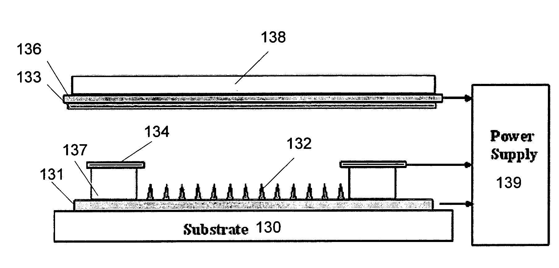
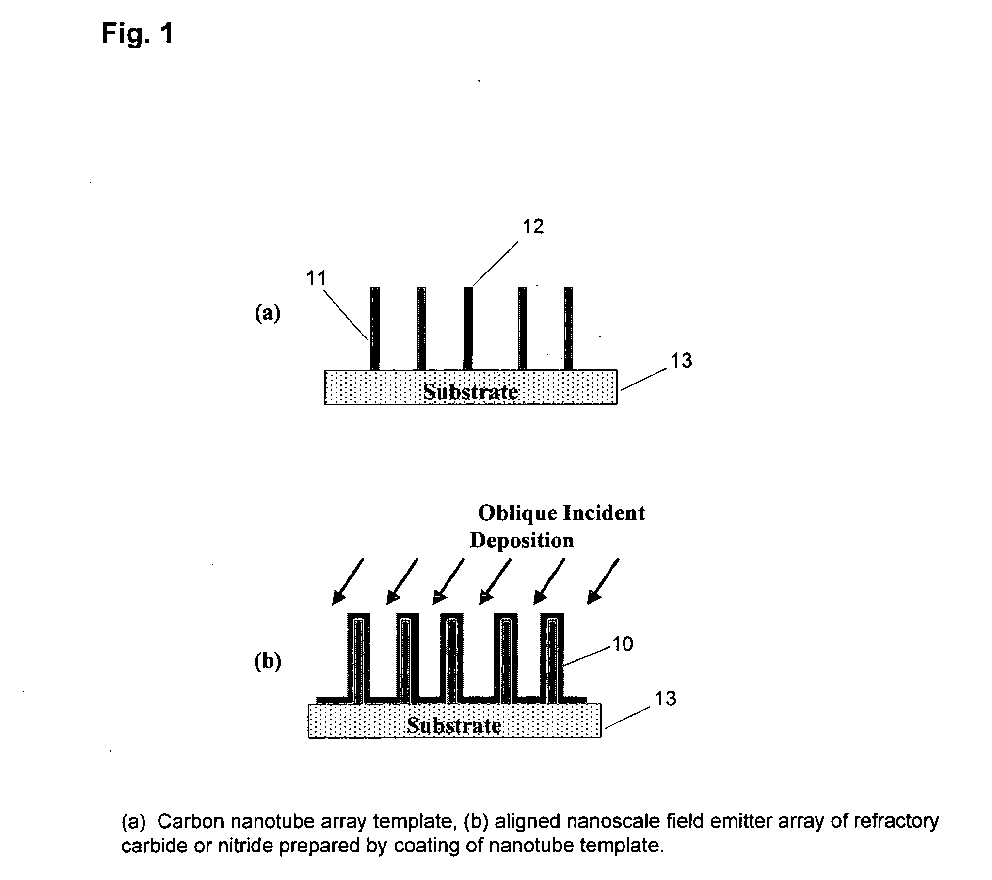
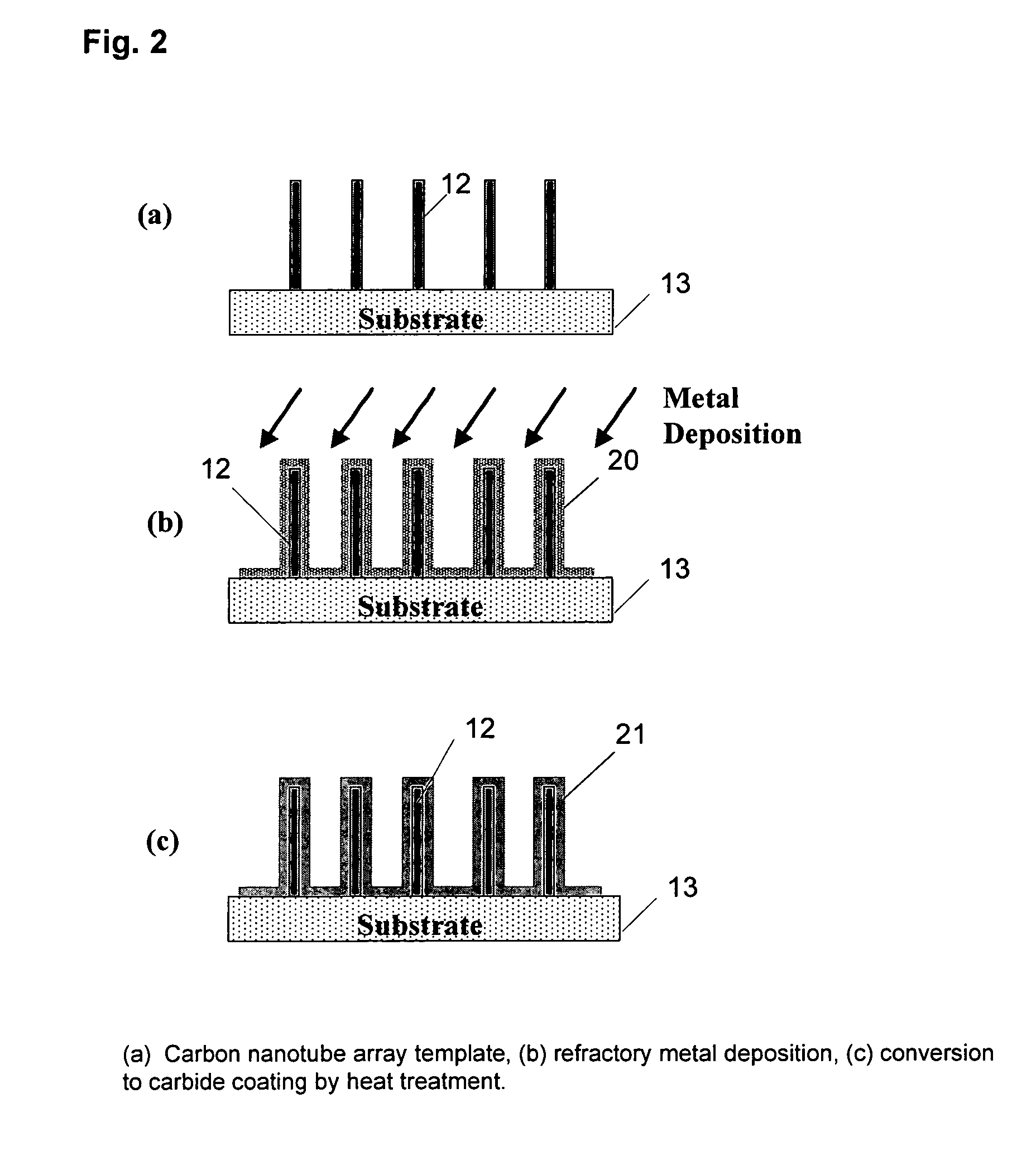
[0030]For efficient field emission of electrons, a high concentration of electric field is desired so as to allow operation of field emitter at relatively low and practical applied electric fields. Carbon nanotubes (CNT) are generally considered as one of the best electron field emitters is because of their high aspect-ratio geometry and resultant electric field concentration which allows significant electron emission at relatively low applied fields. However, field emission is both a function of the field concentration factor and the work function of the emitter. Carbon nanotubes are not exceptionally good in this respect, with a relatively large work function (φ˜5.0 eV). Carbides and nitrides, especially refractory carbides and nitrides provide even lower work functions than that for CNTs, for example, ˜3.8 eV for TaC and ˜3.3 eV for TiN. Having strong atomic bonding and high melting temperatures, these refractory metal carbides and nitrides are mechanically and thermally very sta...


PUM


Abstract

This invention discloses novel field emitters which exhibit improved emission characteristics combined with improved emitter stability, in particular, new types of carbide or nitride based electron field emitters with desirable nanoscale, aligned and sharped-tip emitter structures.

Description

CROSS REFERENCE TO RELATED APPLICATIONS[0001]This application claims the benefit of two U.S. Provisional applications: 1) Ser. No. 60 / 547,459 filed by Dong-Wook Kim, et al. on Feb. 25, 2004 (“Article Comprising Carbide and Nitride Nano Electron Emitters and Fabrication Method Thereof”) and 2) Ser. No. 60 / 568,643 filed by Dong-Wook Kim, et al. on May 6, 2004 and bearing the same title. Both said provisional applications are incorporated herein by reference.FIELD OF THE INVENTION[0002]This invention relates to carbide and nitride electron field emitter structures, and in particular, to such structures using carbon nanostructures as templates.BACKGROUND OF THE INVENTION[0003]Field emitting devices are useful in a wide variety of applications, such as field emission flat panel displays, microwave power amplifiers, and nano-fabrication tools. See U.S. Pat. No. 6,283,812 by Jin, et al “Process for fabricating article comprising aligned truncated carbon nanotubes” issued on Sep. 4, 2001, a...

Claims


Application Information

Patent Timeline
IPC IPC(8): H01J9/00
CPCH01J9/025H01J29/04H01J31/127H01J2201/3043H01J2201/30434H01J2201/30465H01J2201/30469H01J2201/30484H01J2201/30488
Inventor KIM, DONG-WOOKJIN, SUNGHOYOO, IN-KYUNGCHEN, LI-HAN
Owner RGT UNIV OF CALIFORNIA
Why Eureka
Try Eureka