

Nonvolatile semiconductor memory device and manufacturing method thereof, semiconductor device and manufacturing method thereof, and manufacturing method of insulating film
a semiconductor memory and non-volatile technology, applied in the field of insulating film, can solve the problems of low reliability of a semiconductor device, and achieve the effects of low hydrogen content, high withstand voltage, and low cos
- Summary
- Abstract
- Description
- Claims
- Application Information
AI Technical Summary
Benefits of technology
Problems solved by technology
Method used
Image

Examples
embodiment mode 1
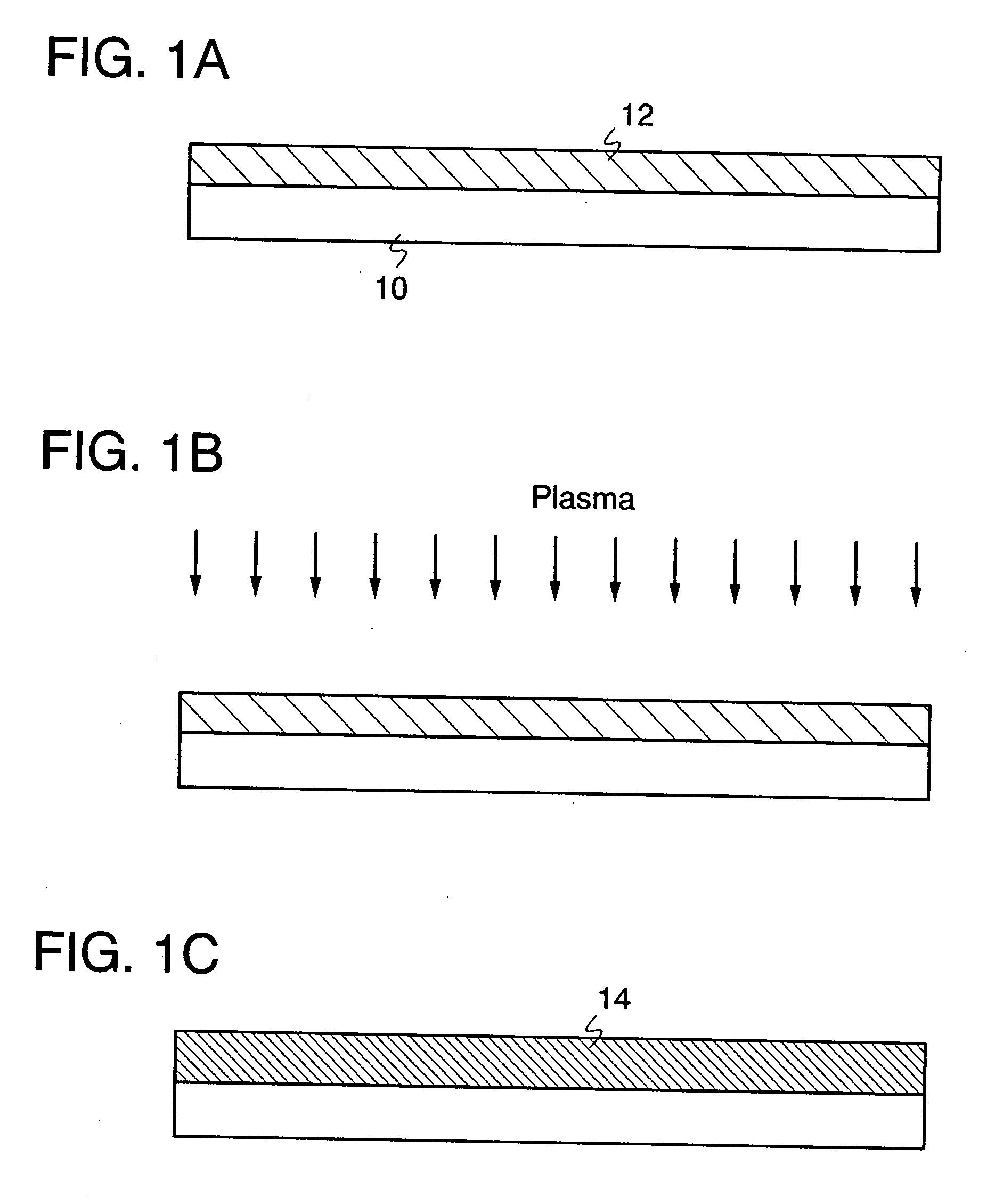
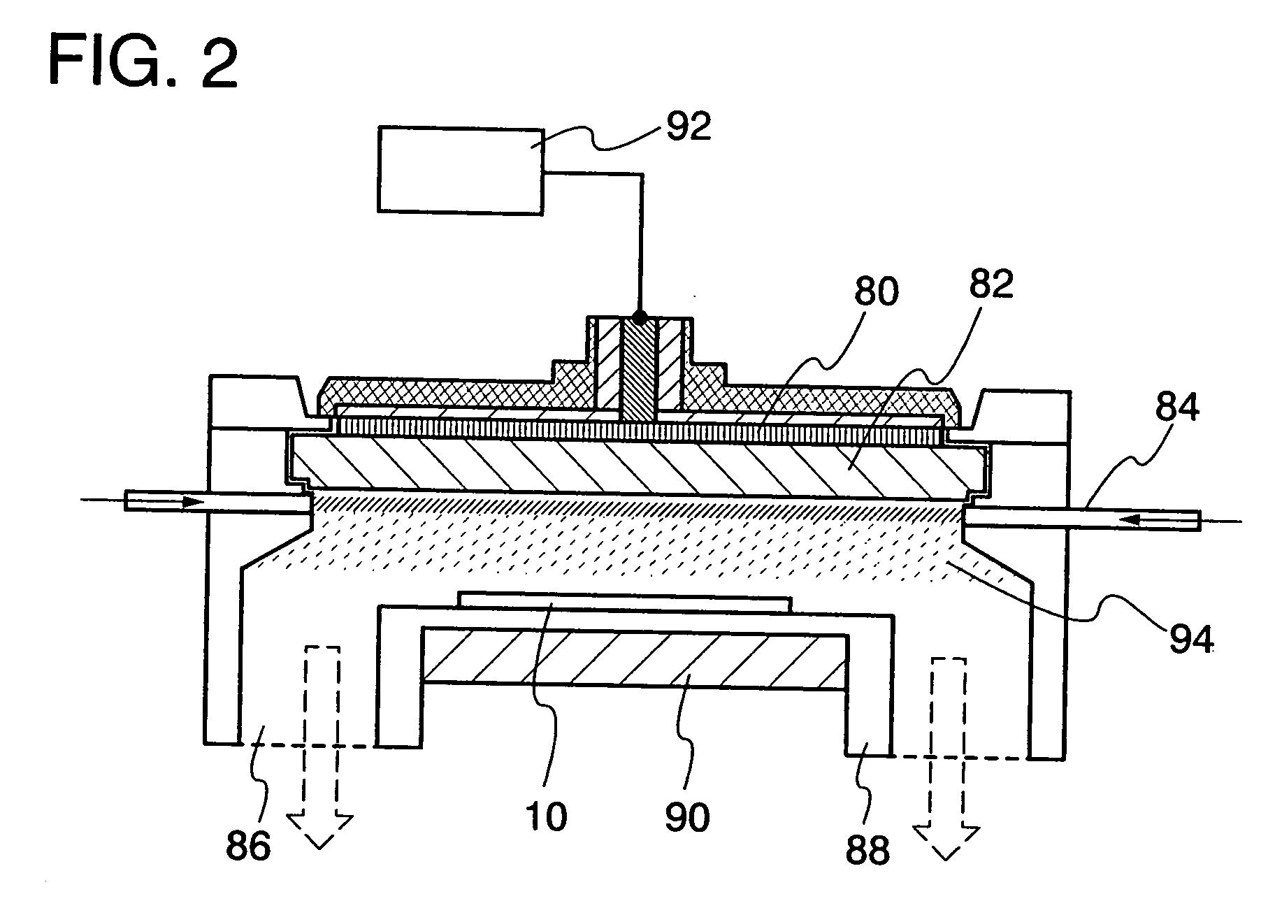
[0077]In the present invention, plasma treatment (plasma oxidation) is performed on an insulating film in an atmosphere including oxygen. Here, an example of performing plasma oxidation on an insulating film formed over a substrate is explained with reference to FIGS. 1A to 1C.
[0078]A first insulating film 12 is formed over a substrate 10 (see FIG. 1A). The substrate 10 may be a glass substrate, a quartz substrate, a sapphire substrate, a ceramic substrate, a metal substrate, or the like. Moreover, these substrates may be provided with a component of a general semiconductor device, such as an insulating film, a semiconductor film, or a gate electrode. In addition, a semiconductor substrate such as a Si substrate, or a semiconductor substrate provided with a component of a general semiconductor device may be used. Further, a plastic substrate made of polyethylene terephthalate (PET), polyethylene naphthalate (PEN), polyether sulfone (PES), acrylic, or the like, or a plastic substrate...
embodiment 1
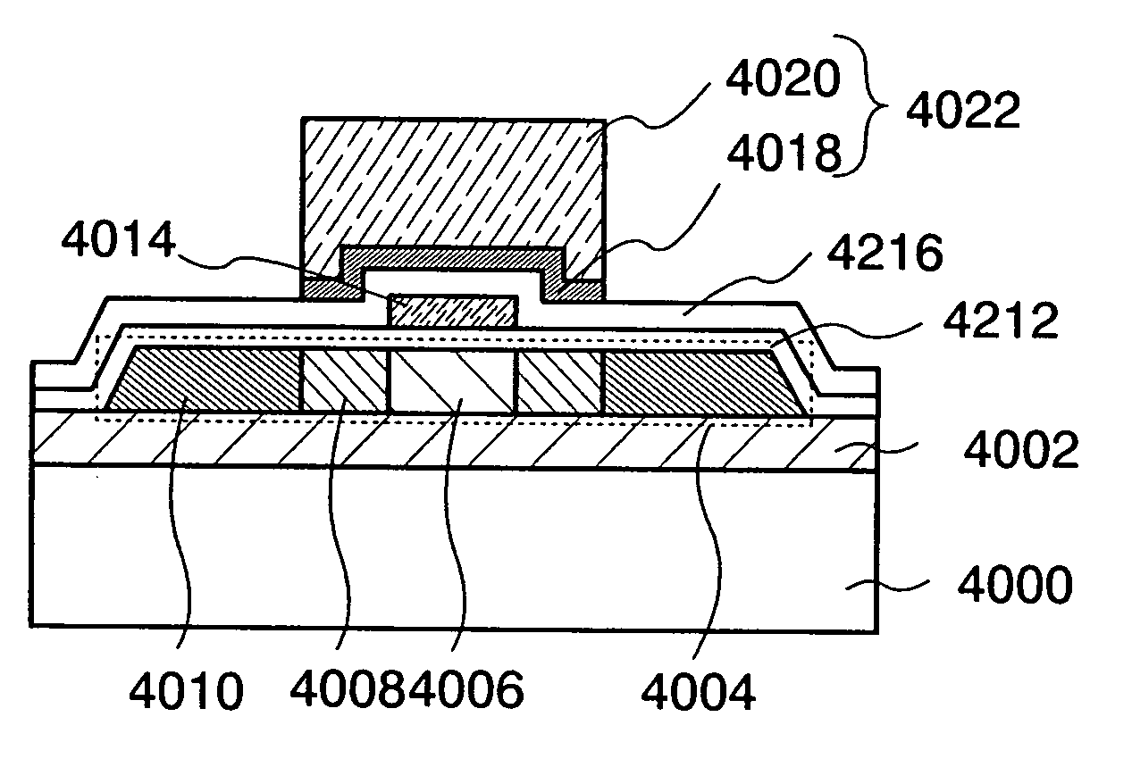
[0097]In this embodiment, an example of a manufacturing method of a semiconductor device using the present invention is explained. Here, description is made of a case of manufacturing a gate insulating film of a thin film transistor (hereinafter also called TFT) by using the present invention. In the structure of the present invention hereinafter explained, a reference numeral indicating the same element is used in common in different drawings, and the description of such an element may be omitted.
[0098]First, a base insulating film 402 is formed over a substrate 400 (see FIG. 4A). The substrate 400 may be a glass substrate, a quartz substrate, a sapphire substrate, a ceramic substrate, a metal substrate, or the like. Moreover, a plastic substrate made of polyethylene terephthalate, polyethylene naphthalate, polyether sulfone, acrylic, or the like can also be used. In addition, a substrate which can withstand at least heat generated in the process can be used. In this embodiment, a ...
embodiment 2
[0131]In this embodiment, a case will be explained in which an insulating film (hereinafter also referred to as a sidewall) is provided at a side surface of the gate electrode in the structure shown in Embodiment 1, with reference to FIGS. 8A to 8E. It is to be noted that the same reference numeral is used to indicate the same part as that in Embodiment 1, and the description of such a part is omitted.
[0132]The steps up to the step shown in FIG. 5B and described in Embodiment 1 are performed (see FIG. 8A).
[0133]Next, an impurity element is added to the semiconductor film 404 by using the gate electrode 418 as a mask, whereby a pair of first impurity regions 822 is formed. The impurity regions 822 formed here function as low-concentration impurity regions (also called LDD regions) of a transistor to be completed later. As the impurity element, an impurity element imparting n-type conductivity or an impurity element imparting p-type conductivity is used. As the impurity element impart...
PUM
| Property | Measurement | Unit |
|---|---|---|
| electron density | aaaaa | aaaaa |
| electron density | aaaaa | aaaaa |
| temperature | aaaaa | aaaaa |
Abstract
Description
Claims
Application Information