Photo-cationic polymerizable epoxy resin composition, liquid discharge head, and manufacturing method thereof
a technology of epoxy resin and photocatalytic polymer, which is applied in the field of epoxy resin composition, can solve the problems of reducing resolution properties and/or dimensional controllability, affecting the patterning properties, and affecting the desired shape, etc., and achieves superior storage stability, good level of accuracy, and easy handling
- Summary
- Abstract
- Description
- Claims
- Application Information
AI Technical Summary
Benefits of technology
Problems solved by technology
Method used
Image
Examples
examples 1 and 2
[0073]After resin compositions as shown in Table 1 were prepared and were then each applied (to have a thickness of 20 μm) on a silicon substrate, exposure using an i-line stepper was performed. In this step, the exposure amount was 5,000 J / m2, and a pattern having an opening of 10 μm in diameter was obtained by patterning.
[0074]In addition, methyl isobutyl ketone was used as a coating solvent for the resin composition, and the solid concentrations of the materials shown in Table 1 were adjusted to 55%.
[0075]A series of steps from the application to the development through the exposure of the discharge port pattern (diameter of 10 μm) were sequentially performed for 100 substrates, and the ratio in the discharge port pattern dimension (diameter) of the 1st substrate to the 100th substrate was measured.
TABLE 110-μm diameterPhoto-cationicratio of 1st / 100thMaterialEpoxy resin compositionpolymerization initiatorBasic additivewaferExample 1EHPE (Daicel ChemicalSP-172 (Adeka Corp.)2,6-bis...
example 3
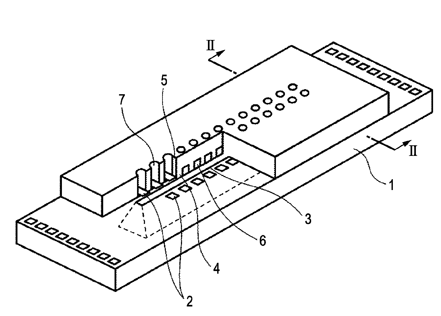
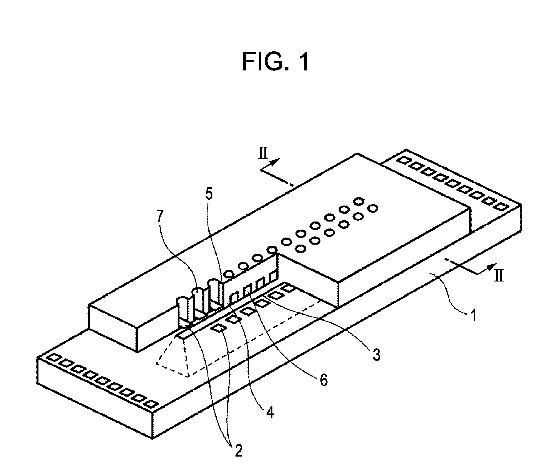
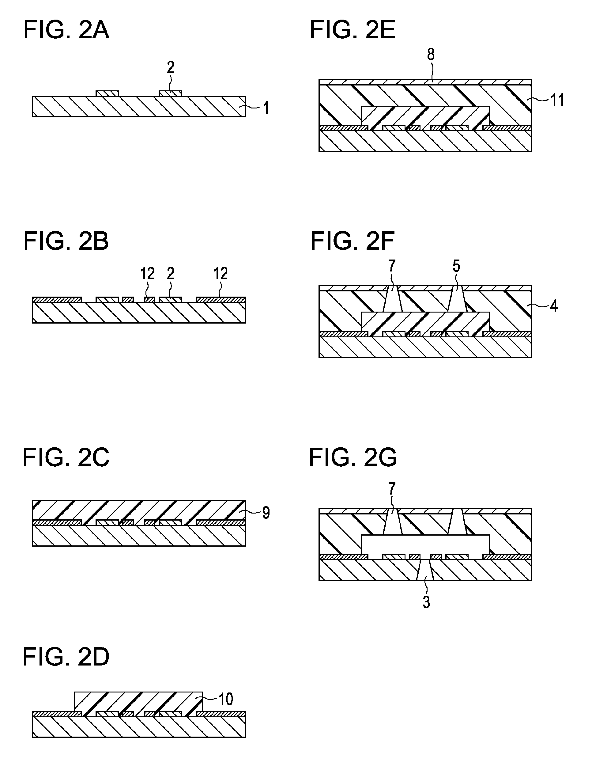
[0077]In this Example, the recording head was formed by the steps shown in FIGS. 2A to 2G.
[0078]First, electrothermal transducers (heater made from HfB2) used as the energy generating elements 2 and the silicon substrate 1 partly provided with an SiN and Ta laminate film (not shown) were prepared (FIG. 2A).
[0079]Next, poly(ether amide) sold under the trade name HIMAL 1200, manufactured by Hitachi Chemical Co., Ltd., was applied on the substrate 1 by a spinner to form the adhesion layer 12 having a thickness of 2.0 μm. Baking was performed in a step-wise manner at 100° C. for 30 minutes and 250° C. for 1 hour. Subsequently, a film of FH-SP (positive type resist manufactured by Fuji Film Olin Co., Ltd., now known as FUJIFILM Electronic Materials Co., Ltd.) was formed on the poly(ether amide) layer, followed by patterning. In addition, by using the FH-SP pattern as a mask, the poly(ether amide) was patterned by O2 plasma ashing, and finally, the FH-SP used as the mask was ashed away by...
example 4
[0087]As the negative type photosensitive resin 11, the following photo-cationic polymerizable epoxy resin composition was used. In addition, the adhesion layer was formed by the method described below. The recording head was formed in the same manner as that described in Example 1.
Photo-cationic polymerizable epoxy resin composition50percent by weightEHPE (manufactured by Daicel Chemical Industries Ltd.)1,4-HFAB (manufactured by Central Glass Co., Ltd.)10percent by weightSP-172 (manufactured by Adeka Corp.)1percent by weightTAZ-110 (Formula 19) (manufactured by Midori Kagaku Co.,0.5percent by weightLtd.)Methyl Isobutyl Ketone19.25percent by weightDiglyme19.25percent by weightFormula 19Compound used for the adhesion layer 12:Poly(ether amide) resin having the following repeating unit20percent by weightand a molecular weight Mw of 25,000Cross-linking agent; hexamethoxymethylmelamine E-21512percent by weight(manufactured by Sanwa Chemical Co., Ltd.)Photo polymerization initiator Sp-17...
PUM
| Property | Measurement | Unit |
|---|---|---|
| Nanoscale particle size | aaaaa | aaaaa |
| Fraction | aaaaa | aaaaa |
| Diameter | aaaaa | aaaaa |
Abstract
Description
Claims
Application Information


