Photomask blank, resist pattern forming process, and photomask preparation process

a pattern forming and resist technology, applied in the field of resist pattern forming process, can solve the problem of difficult control of in-plane uniformity of line width (cd uniformity), and achieve the effect of high in-plane accuracy and in-plane uniformity of line width

Inactive Publication Date: 2008-12-11
SHIN ETSU CHEM IND CO LTD
View PDF15 Cites 17 Cited by
  • Summary
  • Abstract
  • Description
  • Claims
  • Application Information

AI Technical Summary

Benefits of technology

[0025]Also, the resist pattern forming process of the invention is suited in forming a resist pattern from a resist film deposited on a photomask blank as a typical workpiece. By etching the photomask blank through the resist pattern resulting from the process as an etching mask, a photomask with a high in-plane accuracy can be produced.
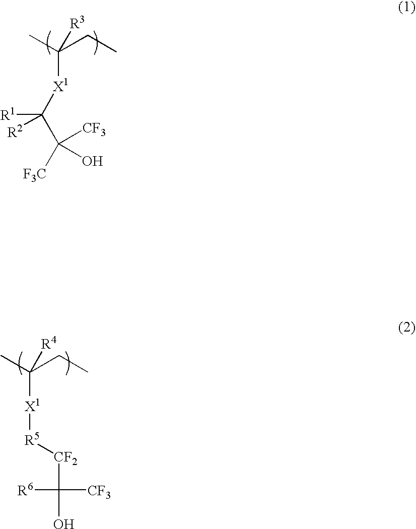
[0029]The polymer (D), specifically the polymer (D) which functions such that the contact angle with neutral water of a resist film comprising components (A) to (D) is larger than the contact angle of a resist film comprising components (A) to (C) and free of component (D) is used as one component of the resist composition to be applied to a photomask blank. The polymer (D) serves to increase the contact angle with pure water of the resist film without exacerbating the pattern profile, resulting in improved in-plane uniformity of line width (or CD uniformity) at the end of mask fabrication.

Problems solved by technology

A tradeoff arises between these problems.
In particular, it is difficult to control the in-plane uniformity of line width (CD uniformity) because the CD uniformity can be affected by almost all steps (e.g., resist coating, storage after coating, EB image writing, PEB, development, and etching) involved in the mask fabrication.

Method used


Image

  • Photomask blank, resist pattern forming process, and photomask preparation process
  • Photomask blank, resist pattern forming process, and photomask preparation process
  • Photomask blank, resist pattern forming process, and photomask preparation process

Examples


example

[0676]Examples and Comparative Examples are given below by way of illustration and not by way of limitation.

Preparation of Polymers

[0677]Polymers or polymeric additives as component (D) to be added to resist compositions were synthesized by a process including selection of suitable monomers, copolymerization in isopropyl alcohol medium, crystallization in hexane, repeated washing with hexane, isolation, and drying. The composition of these polymers was analyzed by 1H-NMR, and the weight average molecular weight (Mw) and dispersity (Mw / Mn) determined by gel permeation chromatography (GPC).

Preparation of Resist Compositions

[0678]Resist compositions were prepared in accordance with the formulation shown in Table 1. The values in Table 1 are expressed in parts by weight (pbw). The components shown in Table 1 are identified below.[0679]Polymers 1 to 6: as described above[0680]Polymer 7: hydroxystyrene-4-(1-methoxy-2-methoxy)hydroxystyrene copolymer[0681]Polymer 8: hydroxystyrene-acetoxys...


PUM

PropertyMeasurementUnit
sizeaaaaaaaaaa
mol %aaaaaaaaaa
mol %aaaaaaaaaa

Abstract

A photomask blank has a resist film comprising (A) a base resin, (B) an acid generator, and (C) a basic compound. The resist film further comprises (D) a polymer comprising recurring units having a side chain having a fluorinated hydrocarbon group which contains a carbon atom to which a hydroxyl group is bonded and vicinal carbon atoms bonded thereto, the vicinal carbon atoms having in total at least two fluorine atoms bonded thereto. Addition of polymer (D) ensures uniform development throughout the resist film, enabling to form a resist pattern having high CD uniformity.

Description

CROSS-REFERENCE TO RELATED APPLICATION[0001]This non-provisional application claims priority under 35 U.S.C. §119(a) on Patent Application No. 2007-150130 filed in Japan on Jun. 6, 2007, the entire contents of which are hereby incorporated by reference.TECHNICAL FIELD[0002]This invention relates to a process for forming a resist pattern by lithography using high-energy radiation such as UV, deep-UV, electron beam, x-ray, excimer laser, gamma-ray or synchrotron radiation, and especially beam lithography, a process for preparing a photomask using the resist pattern formed thereby, and a photomask blank having a chemically amplified positive resist film deposited thereon to which the foregoing processes are advantageously applicable so that the blank is processed into a photomask.BACKGROUND ART[0003]The recent trend toward higher integration in the integrated circuit technology poses a demand for finer feature size patterns. Acid-catalyzed chemically amplified resists are thought promi...

Claims


Application Information

Patent Timeline
Patent Type & Authority Applications(United States)
IPC IPC(8): G03F1/00G03F7/20C08F16/14C08F20/10G03F1/20G03F1/50G03F7/004G03F7/039H01L21/027
CPCG03F1/14G03F7/0392G03F7/0046G03F1/50G03F1/62
Inventor KOITABASHI, RYUJIWATANABE, SATOSHITAKEDA, TAKANOBUMASUNAGA, KEIICHIWATANABE, TAMOTSU
Owner SHIN ETSU CHEM IND CO LTD
Why Eureka
Try Eureka