Silicon wafer having good intrinsic getterability and method for its production

a technology of monocrystalline silicon and intrinsic getterability, which is applied in the direction of silicon compounds, instruments, and under a protective fluid, can solve the problems of damage to the protective oxide of the memory cell, damage to the function of the electronic components fabricated thereon, and damage to the surface of the wafer

Active Publication Date: 2008-12-18
SILTRONIC AG
View PDF7 Cites 13 Cited by
  • Summary
  • Abstract
  • Description
  • Claims
  • Application Information

AI Technical Summary

Problems solved by technology

If special precautions are not taken, then the defects will also be found on the surface of the wafers where they can detrimentally affect the function of the electronic components fabricated thereon.
These depressions lead to problems, for example short circuits on the so-called gate oxide of a CMOS transistor, since defective growth of this surface oxide takes place at this position.
Vertical “trenches”, which are produced by anisotropic etching and are part of a typical CMOS memory cell, may also be short circuited by a COP lying between them, or the protective oxide of the memory cell may be compromised.
Wafers with a high density of OSF seeds present the following disadvantages with respect to reduced component yields: (1) metals are preferentially bound to OSFs (“gettered”), which leads to degradation of the gate oxide due to enhanced formation of nucleation centers for volatile SiO; (2) OSF seeds grow in component-specific thermal processes to form large precipitates, which crucially weaken the silicon matrix due to formation of dislocation loops.
This can lead to enhanced deformation (“warp”) of the silicon wafer, which then in turn interferes with the photolithography step used in the CMOS process since the critical minimum structure linewidths are no longer achieved; (3) large oxygen precipitates, which are caused by OSF seeds, cannot generally be eliminated so as to form a BMD-free zone even by a thermal process, and thus they remain as defects in the active component zone.
This, as already described for COPs, may lead to short circuits in the trench capacitor memory cell, or may weaken its capacitance.
In silicon single crystals, agglomerates of interstitials lead to dislocation loops with extents of several micrometers, which likewise has a detrimental effect on the function of the components produced there.
On the one hand this is desirable since oxygen precipitates on the wafer surface can lead to functional impairment or failure of the relevant components.
On the other hand, however, oxygen precipitates bind metal impurities which diffuse into the silicon wafer during the production of electronic components.
For instance, the oxygen precipitates grow stress-free in zones with a vacancy excess by absorption of vacancies, which is not possible in zones with an excess of interstitials.
More rapid growth is therefore possible in the vacancy-rich zones, and a mixture of zones with an excess of interstitials and zones with an excess of vacancies is generally undesirable on a wafer.
Another problem, however, occurs during the heat treatment of silicon wafers, in the entire volume of which crystal lattice vacancies are the prevalent point defect type and which at the same time are free of agglomerates of crystal lattice vacancies: If the interstitial oxygen concentration [Oi] is selected to be high enough in order to ensure sufficient BMD formation and therefore sufficient getterability, then interfering OSF seeds are formed during the crystal growth when cooling.
If, however, the interstitial oxygen concentration [Oi] is selected to be so low that no OSF seeds are formed during the growth of the crystal, then this leads to no BMD density or a low BMD density which is not enough to achieve a sufficiently large getter effect (for example defined with the aid of the size and density of the BMDs according to Sueoka et al., ELECTROCHEM.

Method used


Image

  • Silicon wafer having good intrinsic getterability and method for its production
  • Silicon wafer having good intrinsic getterability and method for its production
  • Silicon wafer having good intrinsic getterability and method for its production

Examples


example

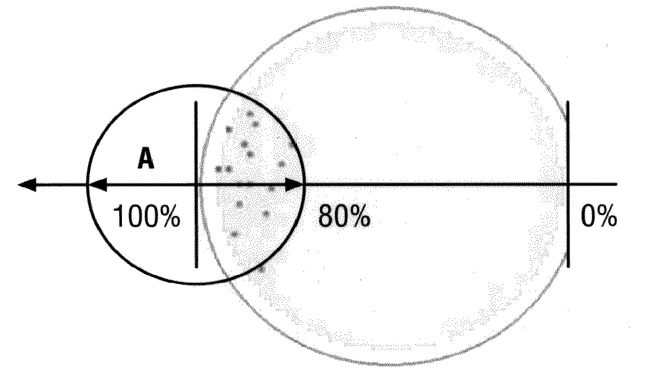
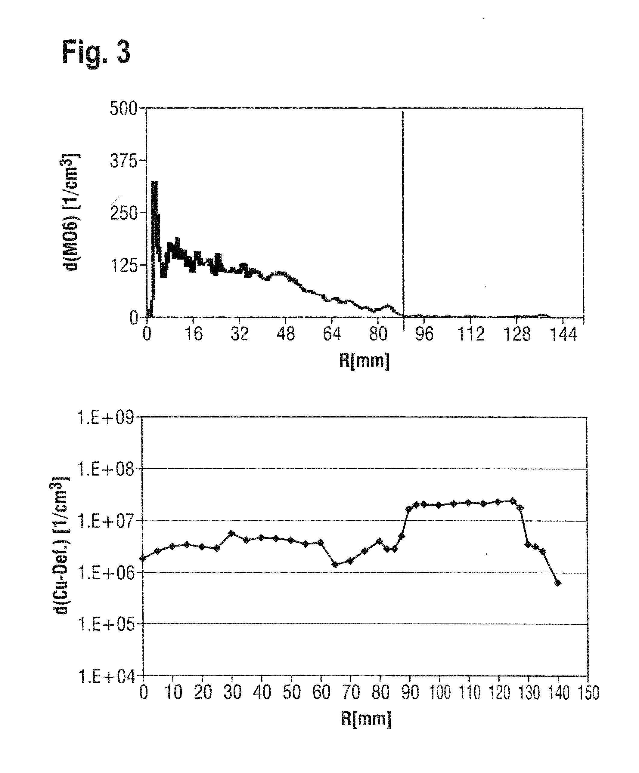
[0084]A silicon single crystal was pulled according to the invention by means of the CZ method and cut into wafers according to the prior art. Four wafers at different rod positions were subjected to the heat treatment according to the prior art. Either these wafers revealed the described COP disk in the measurement with MO6, or they were COP disk-free and according to the Cu decoration technique revealed defects over the entire wafer or at least in zone of 80% of the radius, as measured from the wafer edge (FIG. 14). The heating rates for the heat treatment were selected as follows: 500-700° C.: 5 K / min; 700-900° C.: 4 K / min; 900-1000° C.: 3.5 K / min; 1000-1050° C.: 2 K / min; 1050-1100° C.: 1 K / min. The cooling rates corresponded to the heating rates indicated for the respective temperature ranges.

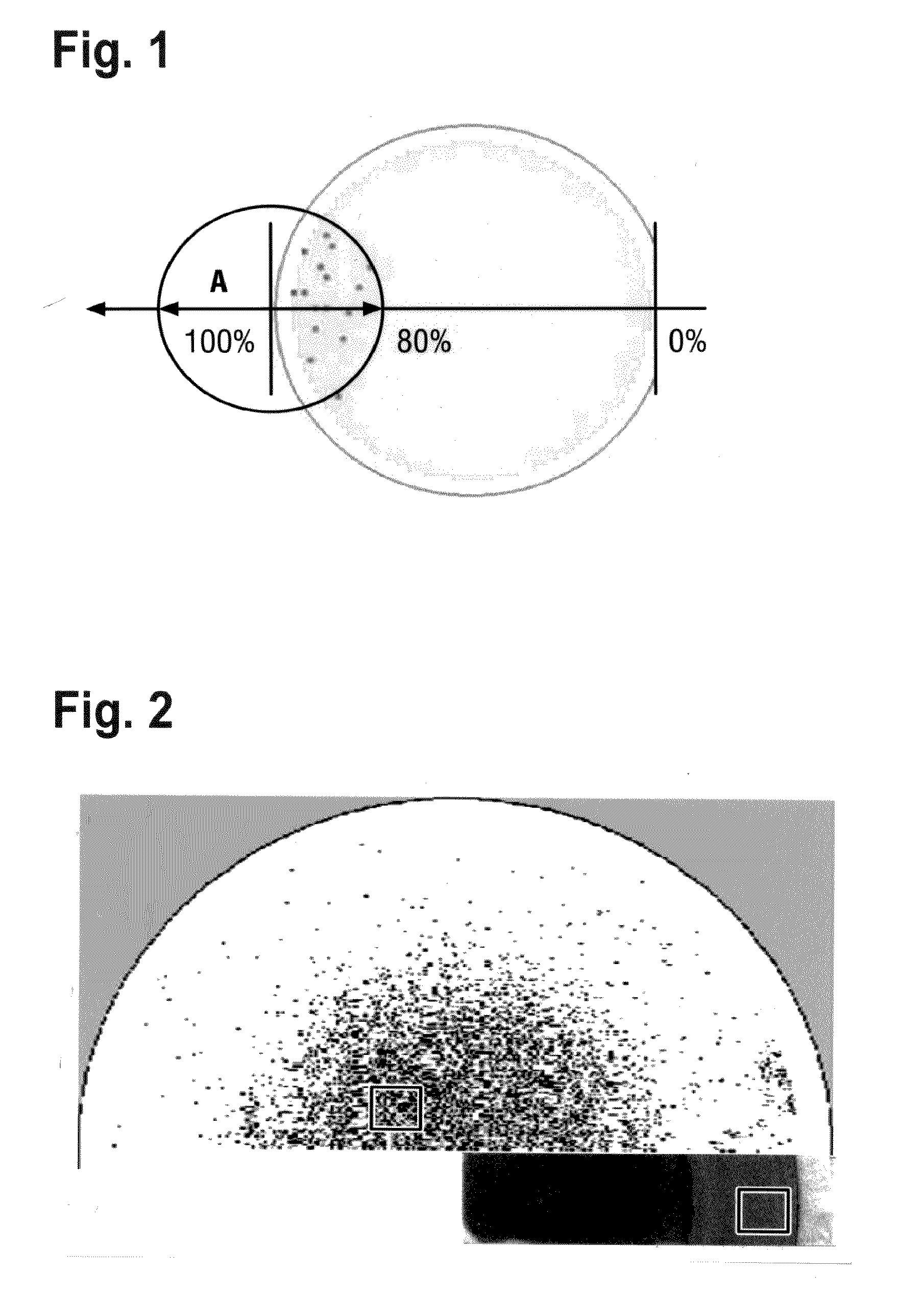
[0085]FIG. 15 shows the result of a radial BMD measurement by means of SIRM. The left-hand value in the legend stands for the interstitial oxygen concentration [Oi] in the silicon wafer bef...


PUM

PropertyMeasurementUnit
sizeaaaaaaaaaa
sizeaaaaaaaaaa
total lengthaaaaaaaaaa

Abstract

Silicon wafers in the entire volume of which crystal lattice vacancies are the prevalent point defect type, have a rotationally symmetric region whose width is at least 80% of the wafer radius, crystal lattice vacancy agglomerates of at least 30 nm in a density ≦6·103 cm−3, crystal lattice vacancy agglomerates of from 10 nm to 30 nm in a density of 1·105 cm−3 to 3·107 cm−3, OSF seeds in a density of 0 to 10 cm−2, and an average bulk BMD density of 5·108 cm−3 to 5·109 cm−3, which varies at most by a factor of 10 radially over the entire silicon wafer, and a BMD-free layer on the front side, wherein the first BMD is found at a depth of at least 5 μm and on average at a depth of at least 8 μm.

Description

BACKGROUND OF THE INVENTION[0001]1. Field of the Invention[0002]The present invention relates to a monocrystalline silicon wafer having good intrinsic getterability, the silicon wafer having a high BMD density in the bulk and a BMD-free layer on its surface. The invention also relates to a method for producing such silicon wafers by heat treatment.[0003]2. Background Art[0004]Silicon single crystals, which are generally produced according to the Czochralski crucible pulling method (CZ method), comprise a range of impurities and defects. The single crystals are sliced into wafers, subjected to a multiplicity of processing steps in order to obtain the desired surface quality and, finally, generally used for the production of electronic components. If special precautions are not taken, then the defects will also be found on the surface of the wafers where they can detrimentally affect the function of the electronic components fabricated thereon.[0005]The following defect types generall...

Claims


Application Information

Patent Timeline
Patent Type & Authority Applications(United States)
IPC IPC(8): B32B3/24C01B33/021
CPCC30B15/203C30B29/06Y10T428/24298Y10T428/26C30B33/02H01L21/208
Inventor MULLER, TIMOWEBER, MARTINKISSINGER, GUDRUN
Owner SILTRONIC AG
Why Eureka
Try Eureka