Light-Emitting Diode and Method For Fabrication Thereof

a technology of light-emitting diodes and fabrication methods, which is applied in the direction of semiconductor/solid-state device manufacturing, electrical equipment, semiconductor devices, etc., can solve the problems of unfavorable light-emitting diodes, unfavorable light-emitting, and complicated assembling circuit techniques, so as to enhance the resistance to voltage accidentally applied, reduce yield, and enhance the effect of light extraction efficiency

Inactive Publication Date: 2008-12-25
SHOWA DENKO KK
View PDF7 Cites 26 Cited by
  • Summary
  • Abstract
  • Description
  • Claims
  • Application Information

AI Technical Summary

Benefits of technology

[0050]This invention, by causing the light-emitting diode lamp produced by utilizing the light-emitting diode which encloses the bonding structure composed of compound semiconductor/high resistance layer/electric conductor with a view to enhancing the resistance to the voltage accidentally applied in the reverse direction to be formed by electrically connecting the electric conductor and the electrode placed more toward the substrate side than toward the light-emitting layer and disposed on the compound semiconductor layer side assuming the same type of conductivity as the electric conductor, is enabled to form easily the light-emitting diode lamp excelling in the resistance to the voltage accidentally applied in the reverse direction without deliberately adding electronic parts, such as protective diodes, condensers and resistors, separately.
[0051]This invention, in an LED provided with a compound semiconductor layer containing a light-emitting layer and a GaP substrate disposed on the light-emitting part and rendered optically transparent to the light emitted from the light-emitting part, is enabled to provide an AlGaInP-based compound semiconductor light-emitting device that is formed in nearly the same height as the GaN-based compound semiconductor light-emitting device without inducing a decrease of yield.
[0052]Owing to the use of the GaP substrate which has the surface orientation fall in the (111) or incline within 20° from the (111), this invention is enabled to form irregularities easily in the substrate by wet etching and conseque

Problems solved by technology

This necessity entails a problem that the LED is unduly enlarged for the sake of securing a space for the installation of the electronic parts.
Then, an attempt to increase the number of such electronic parts to be incorporated in the power supply circuit for the purpose of enhancing the electrostatic breakdown voltage to a still better degree entails a problem that the technique for assembling circuits will become complicated and the cost for the fabrication of the LED will inevitably rise.
The conventional technique which seeks to enhance the reverse voltage of an LED by using a protective diode as a simple component and electrically connecting the relevant components in a parallel pattern as described above, however, necessitates a space for disposing the protective diode and suffers the consequently formed LED to enlarge automatically in chip size.
This undeniably renders the process for fabricating the LED complicated.
When the GaP substrate to be used in the light-emitting device of high luminance mentioned above is made to assume the surface of (100) or a surface inclined within 20° from the (100) in the direction of , there ensues a problem that the substrate having a thickness of 100 to 150 μm will suffer from weak mechanical strength and the process of production thereof will incur a decrease in the yield of produ

Method used


Image

  • Light-Emitting Diode and Method For Fabrication Thereof
  • Light-Emitting Diode and Method For Fabrication Thereof
  • Light-Emitting Diode and Method For Fabrication Thereof

Examples


example 1

[0094]This example specifically explains an example of fabricating a light-emitting diode contemplated by this invention.

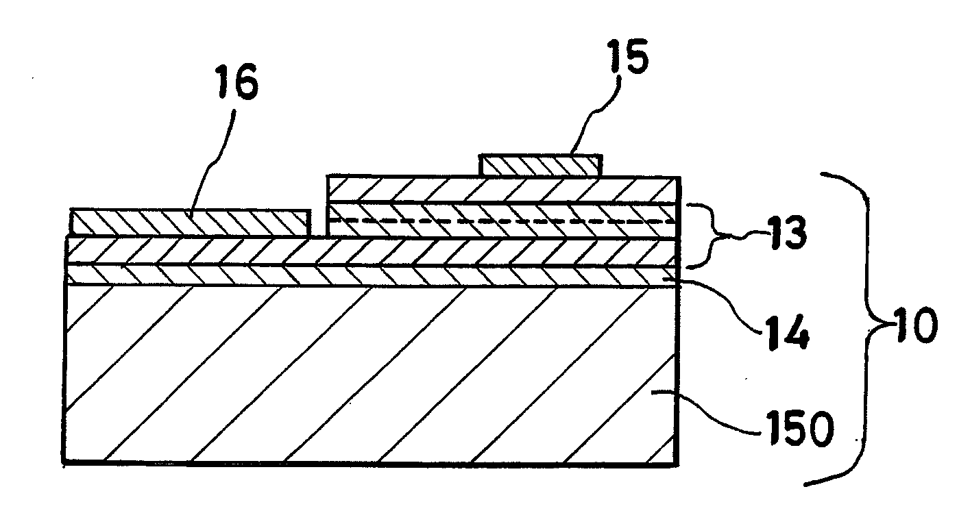
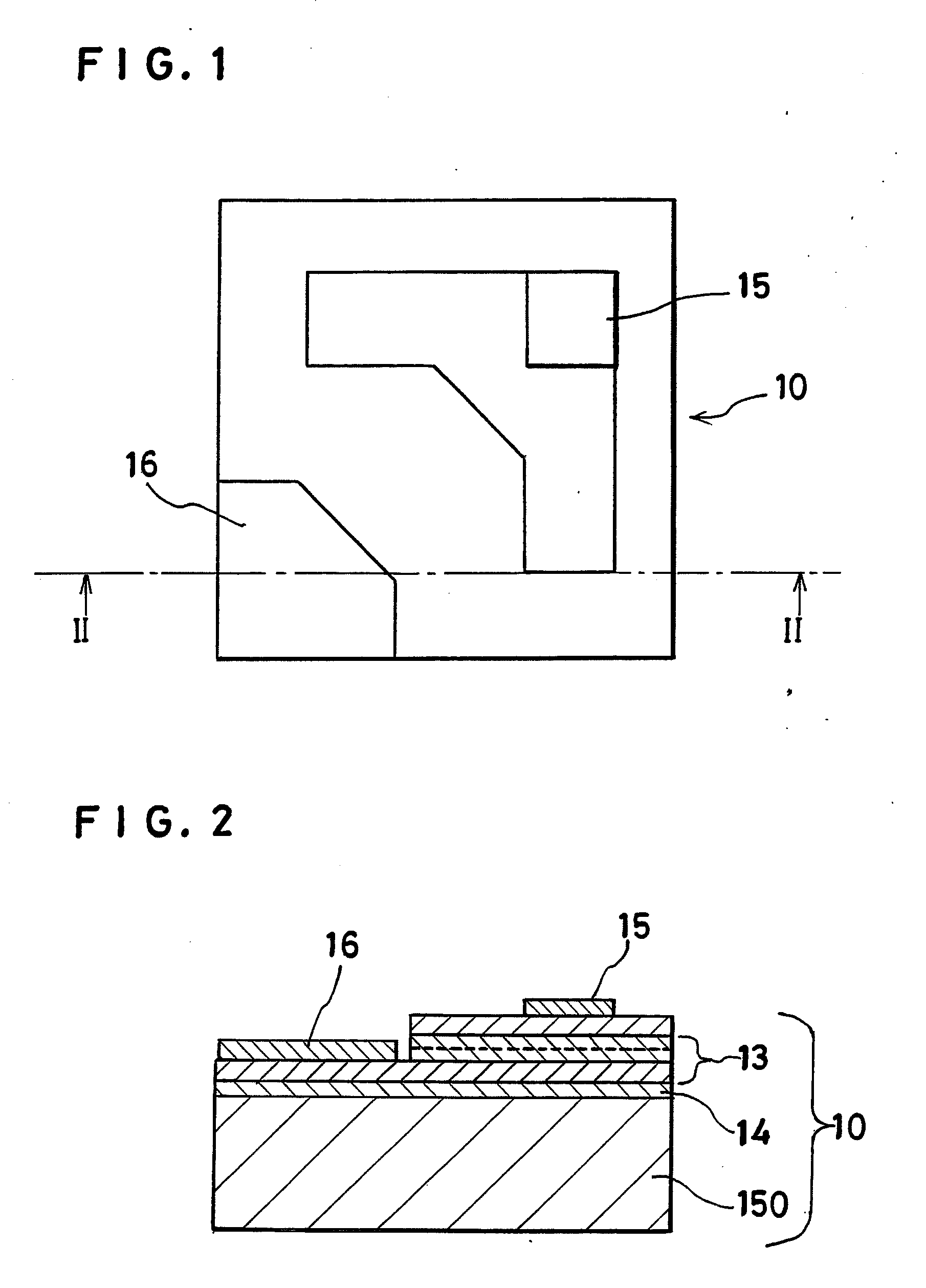
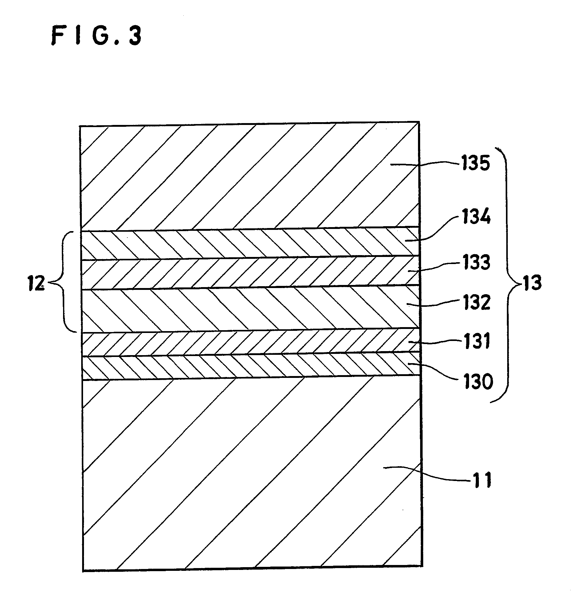
[0095]FIG. 1 and FIG. 2 are diagrams illustrating a semiconductor light-emitting diode that was fabricated in the present example; FIG. 1 representing a plan view thereof and FIG. 2 a cross section taken through FIG. 1 along line II-II. FIG. 3 is a cross section of the layer structure of a semiconductor epitaxial wafer used for the semiconductor diode.

[0096]A semiconductor light-emitting diode 10 fabricated in the present example was a red light-emitting diode (LED) possessing an AlGaInP light-emitting part.

[0097]In this LED, on a semiconductor substrate 11 formed of an Si-doped n-type GaAs single crystal possessing a surface inclined by 15° from the (100), there is formed a semiconductor layer 13 resulting from sequentially stacking a buffer layer 130 formed of a Te-doped n-type GaAs, a contact layer 131 formed of a Te-doped n-type (Al0.5Ga0.5)0.5In0.5P, a lower ...

example 2

[0117]This experiment was performed by following the process of the preceding example while having the electric conductor formed of an n-type SiC having the surface polished to a thickness of 0.1 mm. The amorphous layer had a thickness of about 1 nm.

[0118]The resultant device emitted a light in red color having a main wavelength of 620 nm when the electric current was fed to the p-electrode terminal and the n-electrode terminal. The intensity of light emission at this time was such high luminance as 520 mcd. The forward voltage (Vf: at 20 mA) during the flow of an electric current of 20 mA in the forward direction was about 2.1 V, a fact that reflected good ohmic characteristics of the electrodes.

[0119]In this example, the magnitudes V1=1.5 V, V2=39 V and V3=6 V satisfied the relation of 0.5×V2>V3>2×V1.

[0120]When 30 of the produced lamps were randomly selected as samples and tested for electrostatic breakdown voltage, none of them sustained any breakdown at 100 pF, 1.5 kΩ and 5000 V...

example 3

[0124]This experiment was performed by following the process of Example 1 cited above while having the electric conductor formed of a Zn-doped p-type GaP having a carrier concentration of 9×1018 cm−3. The resultant device, when the electric current was fed to the p-electrode terminal and the n-electrode terminal, emitted a light in red color having a main wavelength of 620 nm. The forward voltage (Vf: at 20 mA) during the flow of an electric current of 20 mA in the forward direction was about 2.1 V, a fact that reflected good ohmic characteristics of the electrodes. The forward voltage (Vf: at 10 μA) was about 1.5 V and the reverse voltage (Vr: at 10 μA) was about 4.5 V. The intensity of light emission at this time was high luminance of 450 mcd. When 30 of the produced lamps were randomly selected as samples and tested for electrostatic breakdown voltage, no breakdown was detected at 100 pF, 1.5 kΩ and 5000 V.

[0125]The reverse voltage (V2: at 10 μA) of the light-emitting part was ab...


PUM


Abstract

A light-emitting diode includes a substrate, a compound semiconductor layer including a p-n junction-type light-emitting part formed on the substrate, an electric conductor disposed on the compound semiconductor layer and formed of an electrically conductive material optically transparent to the light emitted from the light-emitting part and a high resistance layer possessing higher resistance than the electric conductor and provided in the middle between the compound semiconductor layer and the electric conductor. In the configuration of a light-emitting diode lamp, the electric conductor and the electrode disposed on the semiconductor layer on the side opposite to the electric conductor across the light-emitting layer are made to assume an equal electric potential by means of wire bonding. The light-emitting diode abounds in luminance and excels in electrostatic breakdown voltage.

Description

CROSS REFERENCE TO RELATED APPLICATIONS[0001]This application is an application filed under 35 U.S.C. §111(a) claiming the benefit pursuant to 35 U.S.C. §119(e)(1) of the filing dates of Provisional Application No. 60 / 697,959 filed Jul. 5, 2004, No. 60 / 728,325 filed Oct. 20, 2005, No. 60 / 763,927 filed Feb. 1, 2006 and Japanese Patent Application No. 2005-195747 filed Jul. 5, 2005, No. 2005-299599 filed Oct. 14, 2005 and No. 2006-013554 filed Jan. 23, 2006 pursuant to 35 U.S.C. §111(b).TECHNICAL FIELD[0002]This invention relates to a light-emitting diode excelling in electrostatic breakdown voltage and particularly relates to a light-emitting diode of high luminance, a method for the fabrication thereof, and a lamp.BACKGROUND ART[0003]Heretofore, with the object of improving light-emitting diodes in electrostatic breakdown voltage, a large number of methods directed toward improving an LED in breakdown voltage against static electricity by having an electronic part, such as a Zener d...

Claims


Application Information

Patent Timeline
IPC IPC(8): H01L33/00H01L33/30H01L33/02H01L33/42
CPCH01L27/15H01L33/0079H01L33/02H01L2224/45144H01L2924/00H01L2224/48091H01L2224/48227H01L2224/49107Y10S438/936H01L2924/00014H01L33/145H01L33/16H01L2224/48247H01L2224/48465H01L33/0093
Inventor TAKEUCHI, RYOUICHIMATSUMURA, ATSUSHIWATANABE, TAKASHI
Owner SHOWA DENKO KK
Why Eureka
Try Eureka