Organic Thin Film Transistor Array and Method of Manufacturing the Same

a thin film transistor and array technology, applied in the direction of thermoelectric device junction materials, semiconductor devices, electrical apparatus, etc., can solve the problems of disadvantageous method in view of manufacture, significantly low performance, and general increase in manufacturing costs, so as to achieve light weight and thin integrated circuits. , the effect of easy manufacturing

Inactive Publication Date: 2008-12-25
HITACHI LTD
View PDF5 Cites 20 Cited by
  • Summary
  • Abstract
  • Description
  • Claims
  • Application Information

AI Technical Summary

Benefits of technology

[0020]According to the present invention, since an organic CTFT device using an organic TFT can be manufactured, it is possible to easily manufacture a large-area, light-weight and thin integrated circuit using the organic CTFT. The present invention is applicable to liquid crystal displays, organic EL displays, IC cards, and tags.

Problems solved by technology

In addition, since a vacuum apparatus is used in a manufacturing process, manufacturing cost is generally increased.
However, in an organic TFT performance of which can be easily improved is composed of low-molecular-weight molecules, it is common to use vacuum deposition in the manufacturing thereof and the method is disadvantageous in view of the manufacture.
Meanwhile, an organic TFT which can easily suppress manufacturing cost is composed of high-molecular-weight molecules, but it has a significantly low performance and thus is restrictively used.
However, although the property of the bulk can be defined, the electron structure of the semiconductor in the interface between the electrode and the organic semiconductor used in the FET and the interface between the insulator and the organic semiconductor cannot be determined.
In general, since the bond is relatively weak, it can not be applied to the interface between the electrode and the inorganic semiconductor.

Method used


Image

  • Organic Thin Film Transistor Array and Method of Manufacturing the Same
  • Organic Thin Film Transistor Array and Method of Manufacturing the Same
  • Organic Thin Film Transistor Array and Method of Manufacturing the Same

Examples


embodiment 1

[0031]In the present embodiment, the discussion of Physical Review Letters, 84, (26), page 6080 (2000) is extended such that a method of deriving the Schottky barrier Φ from the physical constants of elements configuring the semiconductor and the electrode at the interface between the electrode and the organic semiconductor is derived. Examining the electron state of hydrogen terminated silicon surface-high-molecular polythiophene, gold-pentacene crystal, silver-pentacene crystal, gold-various types of thiol monomolecule film, or silver-various types of thiol monomolecule film, as a combination of the electrode and the organic semiconductor, by electron state measurement using a scanning tunneling microscopy and theoretical computation using first principle calculation, it turned out that the Schottky barrier Φ can be estimated using Equations 7 to 11.

[0032]That is, if the carrier is the electron, the Schottky barrier Φ is given by Equation 7.

Φ=γB(φM−χS)+(1−γB)Eg / 2  Equation 7

[0033]...

embodiment 2

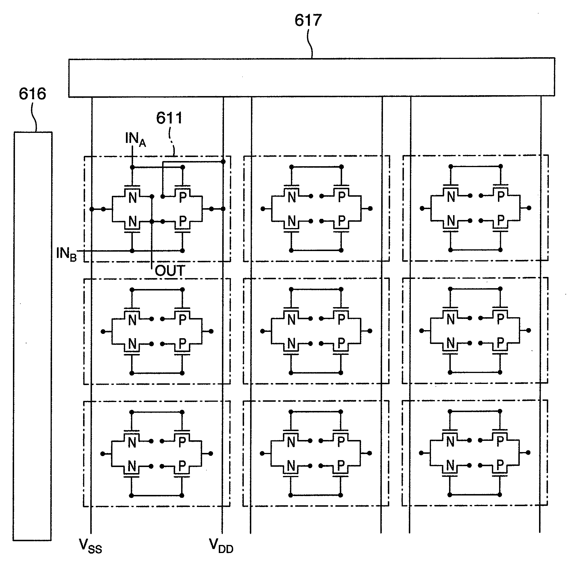
[0041]In the present embodiment, an example of a basic cell of an organic CTFT array according to the present invention is disclosed.

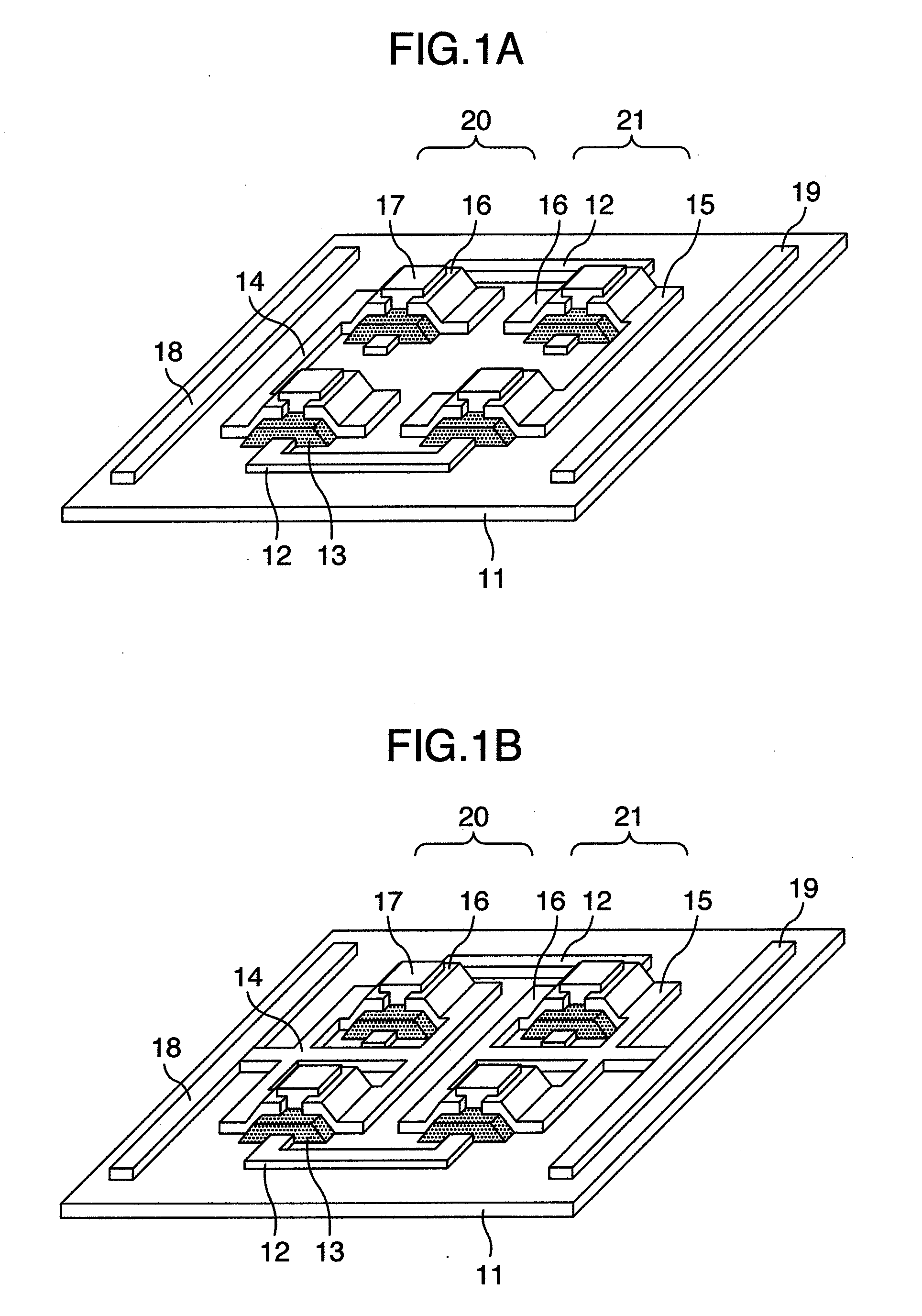
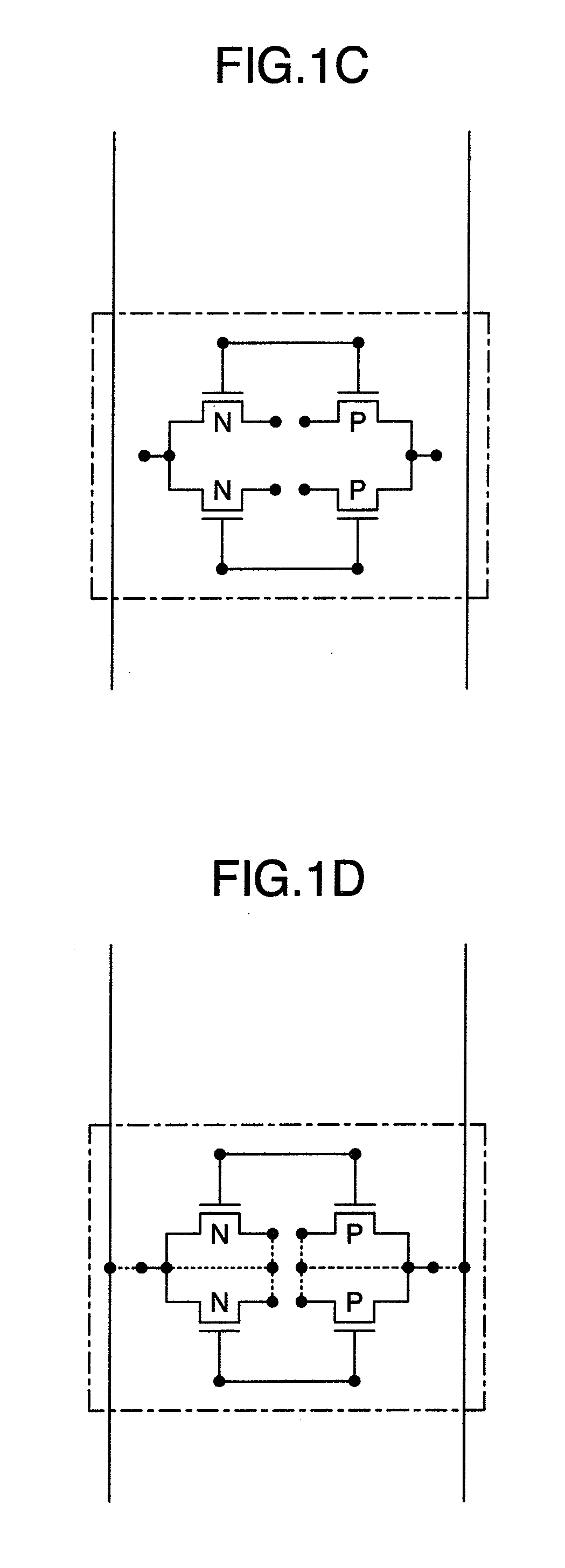
[0042]FIG. 1A is a schematic air view showing an example of the structure of a basic cell of an organic CTFT array according to the present invention. FIG. 2A is a view showing a circuit corresponding to FIG. 1A. In FIG. 1A, an organic semiconductor thin film 17 is a polycrystalline pentacene thin film formed of pentacene crystal particles in the present embodiment. A source electrode 14, a source electrode 15, the organic semiconductor thin film 17, a drain electrode 16 and a gate electrode 12 configure the basic cell. If the organic CTFT is configured, the drain electrodes of one of n-type channel TFTs 20 and one of p-type channel TFTs 21 are connected, the source electrode 15 operates as a ground electrode, the source electrode 14 operates as an operation voltage applying electrode such that a voltage signal is input to the gate electrode 12, and th...

embodiment 3

[0044]In the present embodiment, an example of a method of manufacturing the organic TFT formed by the present invention is disclosed. FIGS. 2A to 2F are cross-sectional views showing an example of the method of manufacturing the organic TFT according to the present invention. In the present embodiment, a material having plasticity is used and the method of configuring the organic TFT of the present invention by a printing method or a coating method without using lithography will be described. FIGS. 2A to 2F are views illustrating the manufacturing method in detail.

[0045]As shown in FIG. 2A, a gate electrode 62 is printed on a plastic substrate 61 using conductive ink. The gate electrode 62 is formed by firing. However, a softening temperature should be careful because plastic is used in the substrate. In the present embodiment, a high-heat-resistance high-transparency polyimide sheet having a thickness 100 μm is used in the substrate 61 and a firing temperature can be increased up ...


PUM


Abstract

An n-type TFT and a p-type TFT are realized by selectively changing only a cover coat without changing a TFT material using an equation for applying the magnitude of a difference in the Fermi energy between an interface of semiconductor and an electrode and between an interface of semiconductor and insulator. At this time, in order to configure a predetermined circuit, the process is performed, as a source electrode and a drain electrode of the p-type TFT and a source electrode and a drain electrode of the n-type TFT being connected all, respectively, and an unnecessary interconnection is cut by irradiating light using a scanning laser exposure apparatus or the like.

Description

INCORPORATION BY REFERENCE[0001]The present application claims priority from Japanese application JP 2007-160862 filed on Jun. 19, 2007, the content of which is hereby incorporated by reference into this application.BACKGROUND OF THE INVENTION[0002]The present invention relates to an organic thin film transistor array and a method of manufacturing the same, and more particularly to an organic complementary thin film transistor (organic CTFT) and a method of manufacturing the same, and more particularly, a desired predetermined circuit configuration using an organic thin film transistor.[0003]In a thin film display device using liquid crystal or an organic electroluminescence (EL) device, a device for driving a pixel, a thin film transistor (TFT) that uses amorphous silicon or polycrystalline silicon for a channel, is used. In a current state, the TFT using amorphous silicon or polycrystalline silicon is unlikely to have plasticity. In addition, since a vacuum apparatus is used in a ...

Claims


Application Information

Patent Timeline
Patent Type & Authority Applications(United States)
IPC IPC(8): H01L51/30H01L21/70
CPCH01L27/283H01L51/0003H01L51/0018H01L51/0021H10K19/10H10K71/12H10K71/233H10K71/60
Inventor HASHIZUME, TOMIHIROSUWA, YUJIFUJIMORI, MASAAKIARAI, TADASHISHIBA, TAKEO
Owner HITACHI LTD
Why Eureka
Try Eureka