Terahertz Electromagnetic Wave Radiation Element and Its Manufacturing Method

a radiation element and electromagnetic wave technology, applied in non-linear optics, instruments, optics, etc., can solve the problems of not yet developing practical elements and short history, and achieve the effect of improving the efficiency of conversion from non-radiation two-dimensional electron plasmon waves to radiation electromagnetic waves and widening the band characteristi

Inactive Publication Date: 2008-12-25
NAT UNIV CORP KYUSHU INST OF TECH (JP) +1
View PDF3 Cites 26 Cited by
  • Summary
  • Abstract
  • Description
  • Claims
  • Application Information

AI Technical Summary

Benefits of technology

[0022]According to the present invention, the efficiency of conversion from non-radiation two-dimensional electro

Problems solved by technology

Studies on application to terahertz devices were started in the 1990's; the

Method used


Image

  • Terahertz Electromagnetic Wave Radiation Element and Its Manufacturing Method
  • Terahertz Electromagnetic Wave Radiation Element and Its Manufacturing Method
  • Terahertz Electromagnetic Wave Radiation Element and Its Manufacturing Method

Examples


example 1

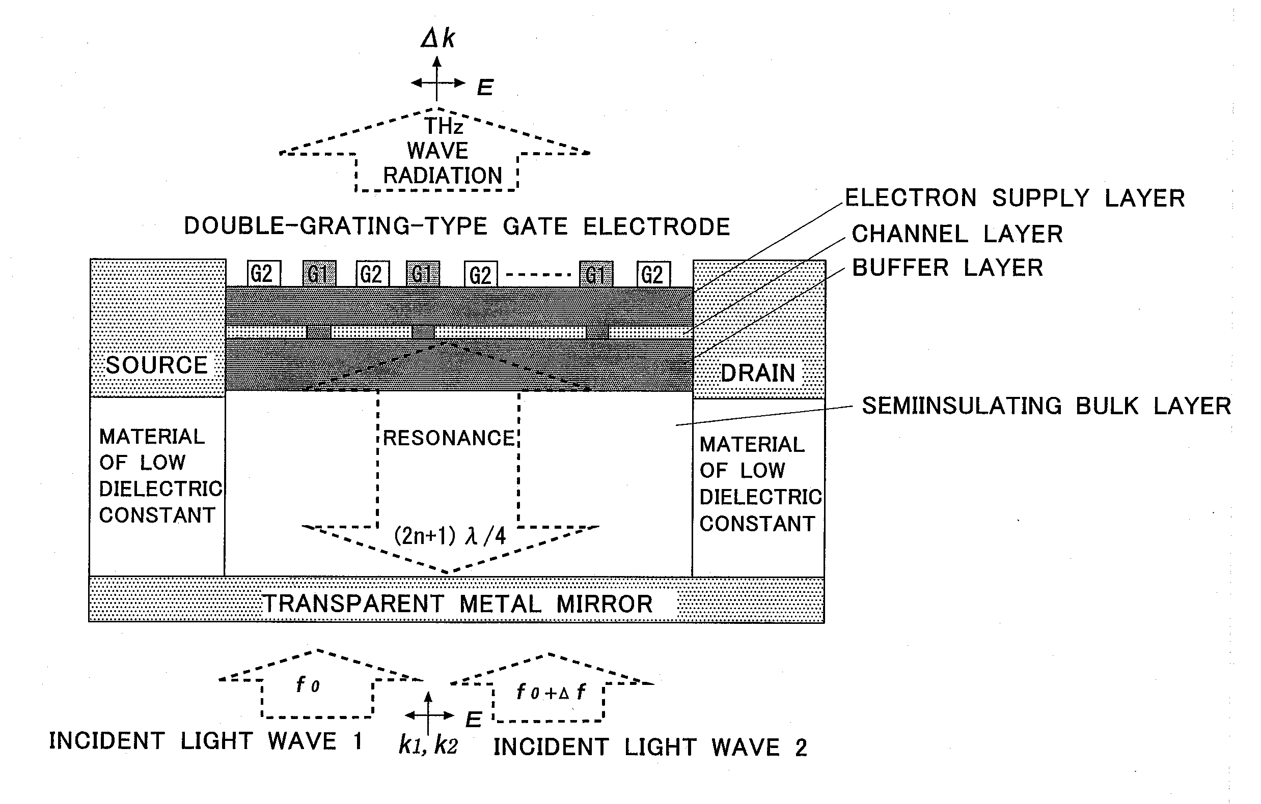
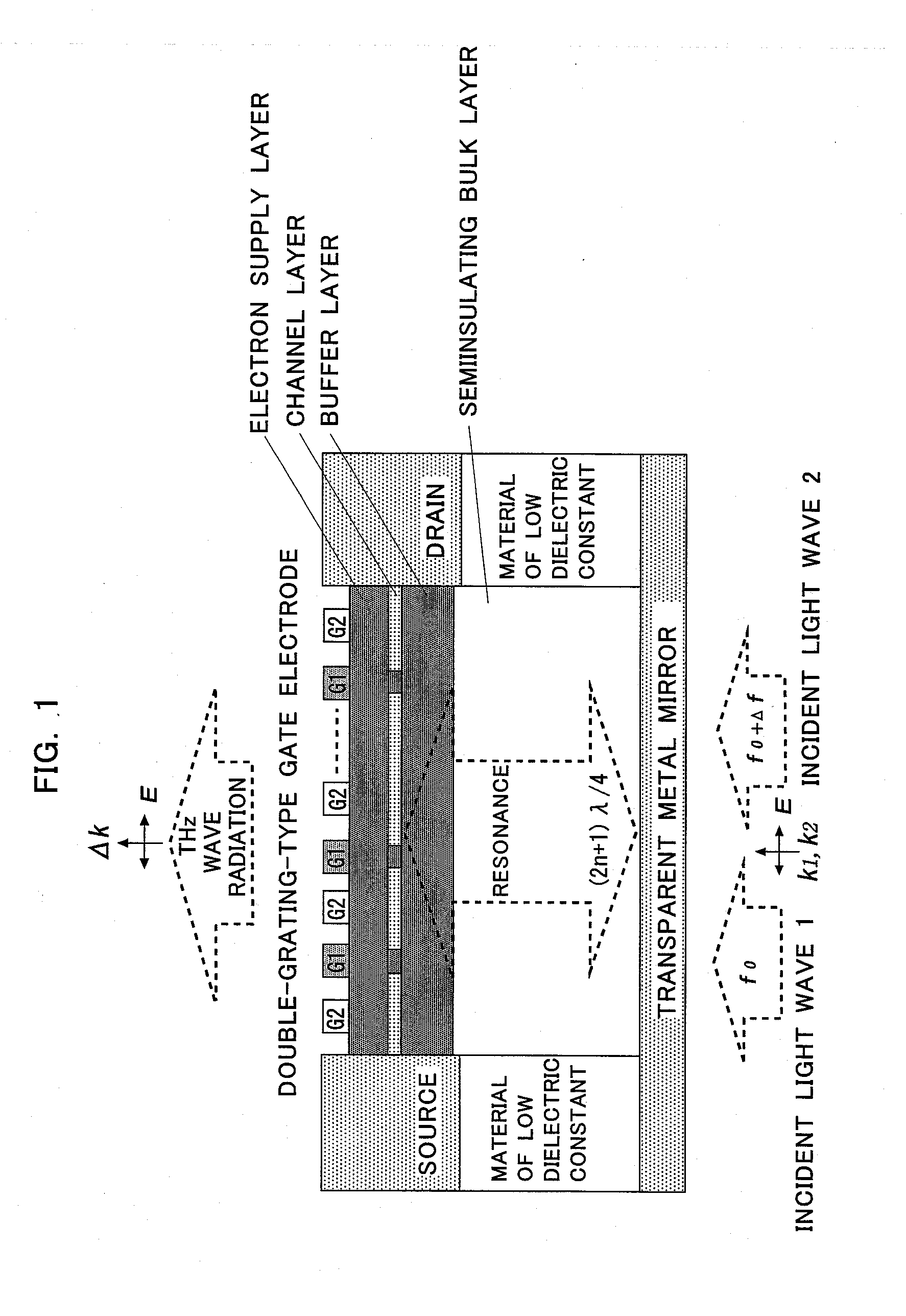
[0045]A specific structural example of the terahertz electromagnetic wave radiation element shown in FIG. 1 will be illustrated. Semiinsulating GaAs (gallium arsenide) is used as a semiconductor bulk layer, and a dielectric material which is lower in dielectric constant than GaAs, such as Si3N4 (silicon nitride), BCB (benzocyclobuten), or polyimide, is used as a clad layer. The semiconductor heterojunction structure is formed through a process of forming a buffer layer on the semiconductor bulk layer by use of, for example, intrinsic GaAs having a wide band gap, forming an electron traveling layer (channel) thereon by use of intrinsic InGaAs having a narrow band gap, and forming a layer of n-type InGaP having a wide band gap thereon. This n-type InGaP layer is a n-type semiconductor containing an excessive amount of electrons, and plays a role of supplying electrons to the electron traveling layer. This is the same mechanism as in ordinary HEMTs (high electron mobility transistors)....

example 2

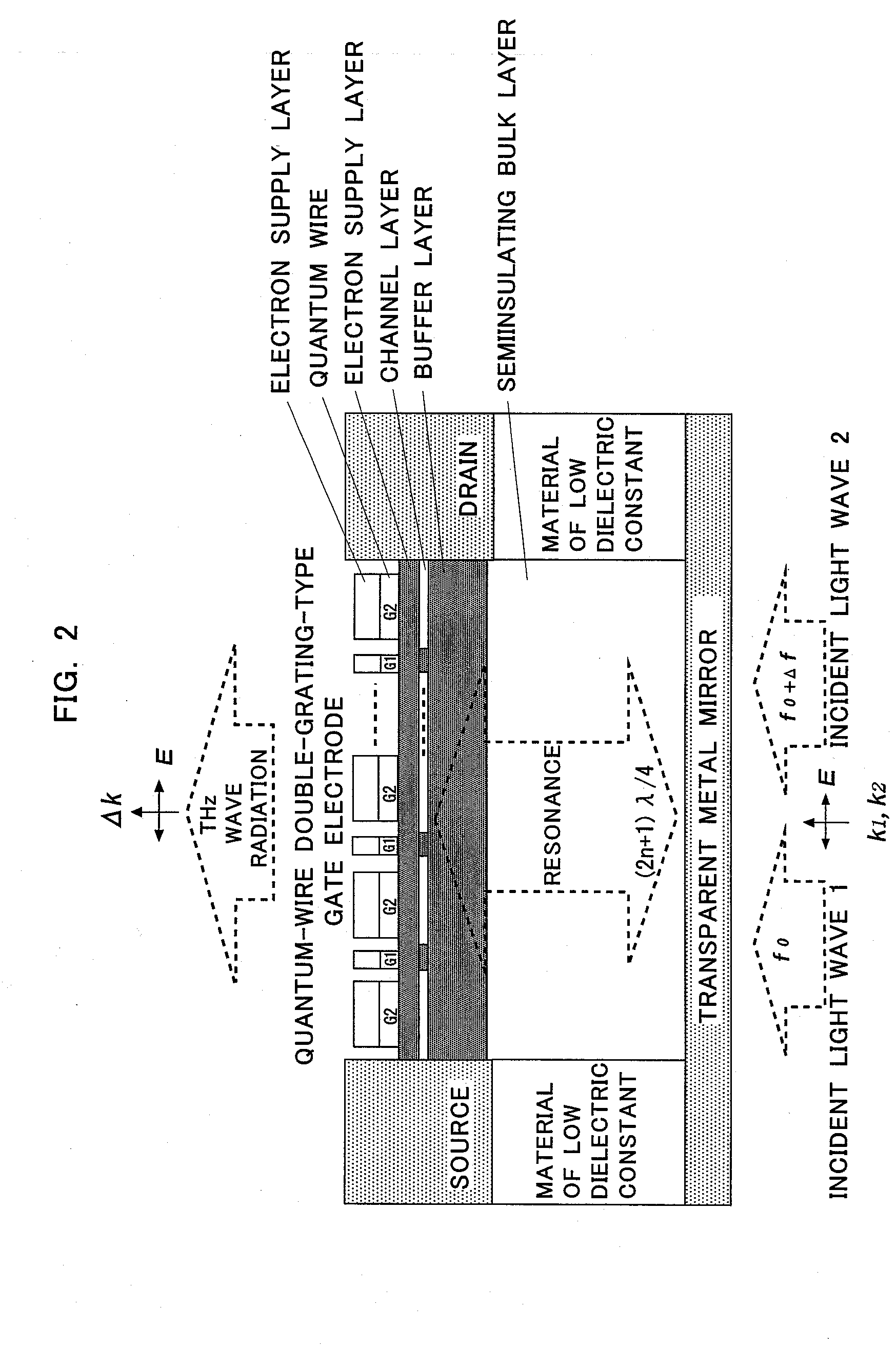
[0047]A structural example different from Example 1 of the terahertz electromagnetic wave radiation element shown in FIG. 1 will be illustrated. The semiconductor heterojunction structure can be formed by use of an InP-based heterojunction structure, the semiconductor bulk layer can be formed by use of semiinsulating InP (indium phosphide), and the clad layer can be formed by use of a dielectric material which is lower in dielectric constant than InP, such as Si3N4 (silicon nitride), BCB (benzocyclobuten), or polyimide. The semiconductor heterojunction structure is formed through a process of forming a buffer layer on the semiconductor bulk layer by use of, for example, intrinsic InAlAs having a wide band gap, forming an electron traveling layer (channel) thereon by use of intrinsic InGaAs having a narrow band gap, and forming thereon a layer of InAlAs in which Si is δ-doped as a donor (doped only in a limited small region in the thickness direction) and which has a wide band gap. T...

example 3

[0048]There will be described the results of a test in which the electron density of the two-dimensional electron layer immediately below the gate gratings was modulated at the cycle of the gate gratings.

[0049]The threshold gate bias at which an electron is inducted in the channel of the electron traveling layer is represented by Vth. For example, in the case of an InP-based device (see Example 2), when the potential of the gate grating A is set to, for example, Vth+0.3 V, and the potential of the gate grating B is set to a higher level; for example, Vth+1.0 V, the channel immediately below the gate grating A has a two-dimensional electron density of 1011 to 1012 cm−2, and the channel immediately below the gate grating B has a high electron density of 1014 cm−2 or higher as in semi-metal. Meanwhile, when the potential of the gate grating B is set to a level lower than that of the gate grating A; for example, Vth−0.2 V, the channel immediately below the gate grating B has a low elect...


PUM


Abstract

The present invention improves the efficiency of conversion from a non-radiation two-dimensional electron plasmon wave into a radiation electromagnetic wave, and realizes a wide-band characteristic. A terahertz electromagnetic wave radiation element of the present invention comprises a semiinsulating semiconductor bulk layer, a two-dimensional electron layer formed directly above the semiconductor bulk layer by a semiconductor heterojunction structure, source and drain electrodes electrically connected to two opposed sides of the two-dimensional electron layer, a double gate electrode grating which is provided in the vicinity of and parallel to the upper surface of the two-dimensional electron layer and for which two different dc bias potentials can be alternately set, and a transparent metal mirror provided in contact with the lower surface of the semiconductor bulk layer, formed into a film shape, functioning as a reflecting mirror in the terahertz band, and being transparent in the light wave band. Two light waves are caused to enter from the lower surface of the transparent metal mirror, and two different dc bias potentials are alternately applied to the double gate electrode grating so as to periodically modulate the electron density of the two-dimensional electron layer in accordance with the configuration of the double gate electrode grating.

Description

TECHNICAL FIELD[0001]The present invention relates to a terahertz electromagnetic wave radiation element which receives two coherent light waves, mixes them, and radiates a terahertz electromagnetic wave corresponding to the difference frequency thereof, and to a method of manufacturing the same.BACKGROUND ART[0002]A two-dimensional electron system is coherently polarized and vibrationally excited by means of an optical phonon or photon corresponding to inter-sub-band energy. This vibrational quantum is called two-dimensional electron plasmon. At a typical two-dimensional electron density (1011 to 1012 cm−2), the two-dimensional electron plasmon is of a wavelength range of micron to submicron, and the basic mode frequency reaches the terahertz band. Therefore, the two-dimensional electron plasmon has a capability of serving as a mechanism for realizing functions of electromagnetic wave oscillation, electromagnetic wave detection, frequency mixing, frequency multiplication, etc. in t...

Claims


Application Information

Patent Timeline
IPC IPC(8): H01L33/00H01L31/00H01L21/00H01S1/02
CPCH01S1/02H01S2302/02G02F1/3534G02F2203/13H01L31/09H01L31/0224H01L31/02327
Inventor OTSUJI, TAIICHISANO, EIICHI
Owner NAT UNIV CORP KYUSHU INST OF TECH (JP)
Why Eureka
Try Eureka