Growth of indium gallium nitride (InGaN) on porous gallium nitride (GaN) template by metal-organic chemical vapor deposition (MOCVD)

a gallium nitride and gallium nitride technology, applied in the direction of crystal growth process, polycrystalline material growth, chemically reactive gas, etc., can solve the problems of low percentage of indium incorporation, phase separation, and impede the growth of indium-rich materials, so as to increase the incorporation

Inactive Publication Date: 2009-01-01
NAT UNIV OF SINGAPORE
View PDF21 Cites 72 Cited by
  • Summary
  • Abstract
  • Description
  • Claims
  • Application Information

AI Technical Summary

Benefits of technology

[0010]It is an object of the present invention to provide a technique to significantly increase indium incorporation and achieve a significant red-shift in the wavelength emission of InGaN.

Problems solved by technology

However, there are problems impeding the progress in the growth of indium-rich InGaN, which include poor optical properties, low percentage of indium incorporation, phase separation, and the formation of indium droplets on the surface.
The growth of InGaN alloys is very challenging, mostly due to the trade off between the epilayer quality and the amount of indium incorporated into the alloy as the growth temperature is changed.
Difficulties in the metal organic chemical vapor deposition (MOCVD) growth of high quality InGaN arise mainly because the InN decomposes at a low temperature of around 500° C. while below 1000° C., the decomposition of ammonia is low.
All these difficulties arise because of the large difference in inter-atomic spacing between GaN and InN which gives rise to a solid phase miscibility gap and limits the equilibrium InN mole fraction in GaN at a particular growth temperature [I. Ho and G. B. Stringfellow, Appl. Phys. Lett. 69, 2701 (1996)].
Beside the problems that arise from the solid phase miscibility gap between GaN and InN, there is still another problem that arises because of the lack of suitable substrates for GaN and its alloy.
Such heteroepitaxy growth typically gives rise to high dislocation density and residual strain as the result of lattice mismatch and thermal expansion coefficient difference, which are detrimental to the electrical and optical properties of GaN-based devices.
Many ways have been investigated to reduce the effects of this problem, though, to date there are still many defects in the epilayer.
Although all the methods described above utilize a porous template to grow a film or epilayer with reduced dislocation density, none has an objective to achieve high indium incorporation in InGaN.

Method used


Image

  • Growth of indium gallium nitride (InGaN) on porous gallium nitride (GaN) template by metal-organic chemical vapor deposition (MOCVD)
  • Growth of indium gallium nitride (InGaN) on porous gallium nitride (GaN) template by metal-organic chemical vapor deposition (MOCVD)
  • Growth of indium gallium nitride (InGaN) on porous gallium nitride (GaN) template by metal-organic chemical vapor deposition (MOCVD)

Examples


Embodiment Construction

[0021]The conventional method of InGaN growth is as follows: first, a low-temperature nucleation layer is grown, followed by growth of a high-temperature GaN layer, with the former usually performed in the range of 450° C. to 600° C., and the latter usually performed in the range of 900° C. to 1100° C., most typically at about 1015° C. to 1030° C. The temperature is next lowered to about 700° C. to 800° C. to grow the InGaN layer.

[0022]According to the invention, it has been found that the main-peak of room temperature photoluminescence from the InxGa1-xN layer is 575 nm with a spectral broadening extending from 480 nm to 720 nm. It shows a significant red-shift and enhancement of intensity as compared to the emission of a InxGa1-xN layer grown by the conventional method with the same growth conditions (including TMIn and TMGa flows, growth temperature, and pressure).

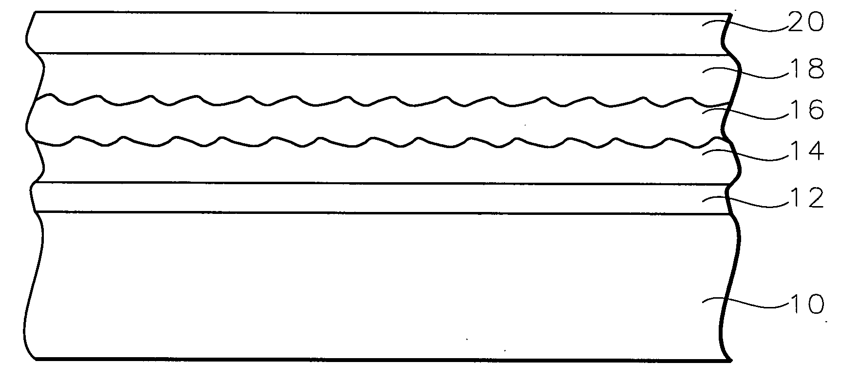
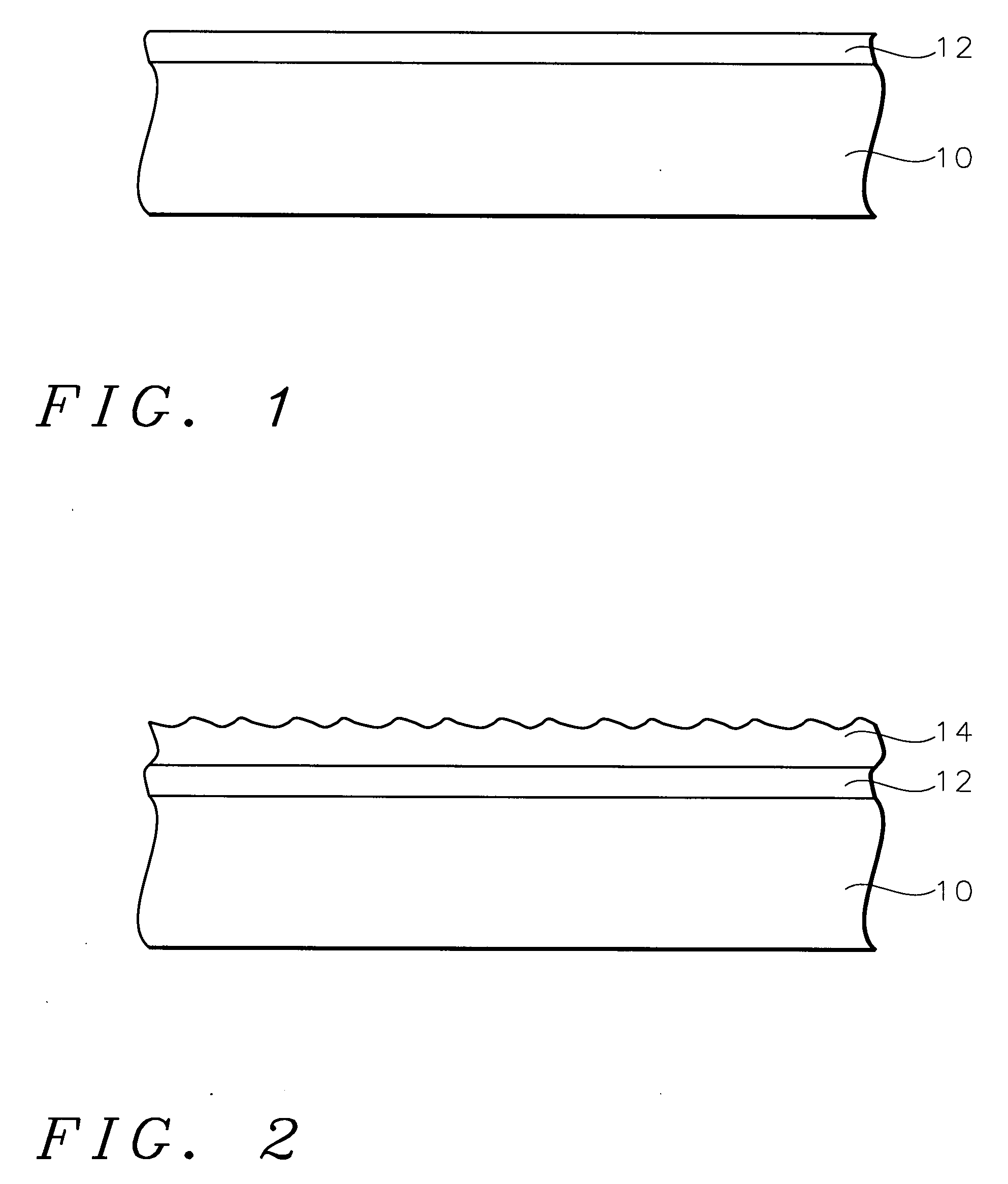
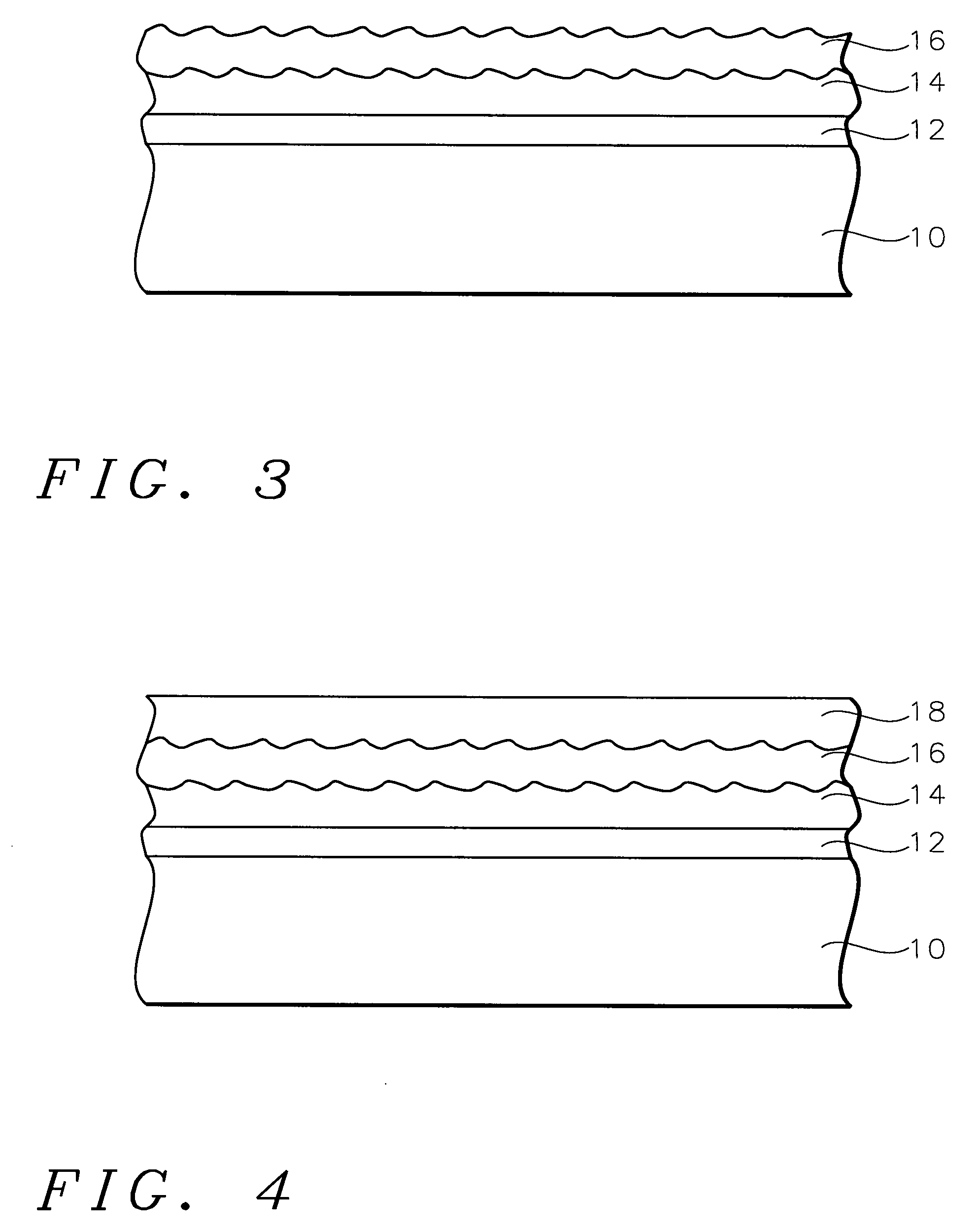
[0023]The porous GaN layer of the present invention acting as the growth template is very important for the quality o...


PUM

PropertyMeasurementUnit
temperatureaaaaaaaaaa

Abstract

Si-doped porous GaN is fabricated by UV-enhanced Pt-assisted electrochemical etching and together with a low-temperature grown buffer layer are utilized as the template for InGaN growth. The porous network in GaN shows nanostructures formed on the surface. Subsequent growth of InGaN shows that it is relaxed on these nanostructures as the area on which the growth takes place is very small. The strain relaxation favors higher indium incorporation. Besides, this porous network creates a relatively rough surface of GaN to modify the surface energy which can enhance the nucleation of impinging indium atoms thereby increasing indium incorporation. It shifts the luminescence from 445 nm for a conventionally grown InGaN structure to 575 nm and enhances the intensity by more than two-fold for the growth technique in the present invention under the same growth conditions. There is also a spectral broadening of the output extending from 480 nm to 720 nm.

Description

FIELD OF THE INVENTION[0001]This invention relates to optoelectronics devices and fabrication methods, particularly to light emitting diodes (LEDs) and laser diodes (LDs).BACKGROUND OF THE INVENTION[0002]Light emitting diodes are widely used in optical displays, traffic lights, data storage, communications, medical and many other applications.[0003]Recent breakthroughs in blue emitting GaN-based LEDs and LDs have attracted much attention on the growth of group III-nitrides, in particular InGaN. InGaN is a very important material because it is used as the active layer of LEDs and LDs. The band gap of InGaN can be varied to provide light over nearly the whole spectral range from near UV to red from the combination of GaN and InN band gap. However, there are problems impeding the progress in the growth of indium-rich InGaN, which include poor optical properties, low percentage of indium incorporation, phase separation, and the formation of indium droplets on the surface. For growing In...

Claims


Application Information

Patent Timeline
Patent Type & Authority Applications(United States)
IPC IPC(8): H01L29/205H01L21/20
CPCC30B25/02C30B29/403H01L21/02389H01L21/02458H01L33/32H01L21/0262H01L21/02658H01L33/0075H01L33/16H01L21/0254
Inventor CHUA, SOO JINHARTONO, HARYONOSOH, CHEW BENG
Owner NAT UNIV OF SINGAPORE
Why Eureka
Try Eureka