Optical clock recovery apparatus and method and birefringent medium

a recovery apparatus and optical clock technology, applied in the field of optical clock recovery apparatus and method, can solve the problems of optical loss, optical signal degradation, waveform degradation in both the temporal and frequency domain,

Inactive Publication Date: 2009-01-01
OKI ELECTRIC IND CO LTD
View PDF3 Cites 11 Cited by
  • Summary
  • Abstract
  • Description
  • Claims
  • Application Information

AI Technical Summary

Benefits of technology

[0033]After diligent research into the problems described above, the inventor found that if the direction of polarization of the input optical signal was perpendicular to the direction of polarization of the recovered optical clock signal, then the recovered optical clock signal could be separated from the components of the input optical signal on the basis of their polarization difference, making it possible to recover an optical clock signal that did not include components of the input optical signal.

Problems solved by technology

With the increasing distances come increased problems of optical signal degradation, including waveform degradation in both the temporal and frequency domains.
The causes are optical loss, signal-to-noise-ratio degradation owing to the use of multiple optical amplifier stages, and waveform distortion owing to group velocity dispersion.
As transmission distances increase, these problems become increasingly apparent.
When the bit rate of an OTDM signal becomes as high as forty gigabits per second (40 Gb / s), at the present state of the art, recovery of an electrical clock signal becomes difficult, because the electronic devices used as optical-to-electric conversion elements and as components of electrical filters lack the operating speed necessary to keep up with the bit rates of multiplexed optical transmission.
A first major problem with the three methods described above is that in addition to a mode-locked laser or a self-pulsating laser they require a wavelength filter with a passband positioned at the lasing wavelength of the laser to remove the wavelength component of the input optical signal from the optical output of the mode-locked laser or self-pulsating laser, as noted by Bao et al. in the second paragraph in the left column of page 3 of the cited reference, and by Brox et al. in the second column of page 2 of the cited reference.
The need for an optical wavelength filter increases the size, number of components, and cost of an all-optical clock recovery device employing any of the above methods.
A more basic problem is that if the input optical signal has the same or nearly the same wavelength as the recovered clock signal, then no wavelength filter can exclude unwanted input optical signal components from the recovered optical clock signal.
With a mode-locked laser, a further problem is that if the input optical signal and the recovered optical clock signal have the same wavelength, or nearly the same wavelength, the operation of the mode-locked laser becomes unstable due to optical injection locking, making it impossible to recover the optical clock signal.
A second major problem with the three methods above is that the optical clock signal recovery apparatus will not operate properly unless special care is taken.
Effective control of optical injection locking enables the frequency and phase of the lasing mode of the mode-locked laser to be controlled, but maintaining the stability of this state is extremely difficult with present control techniques.
As a result, random optical beats arise between the lasing spectrum of the mode-locked semiconductor laser and the wavelength components of the input optical signal, making recovery of a stable optical clock signal difficult.
If optical injection locking could be controlled, it could be used to recover an optical clock signal, but there would still be practical problems, because the lasing spectrum of the mode-locked semiconductor laser would differ considerably, depending on whether the input optical signal was present or absent, as shown by Yokoyama et al. in FIG. 6 in the article ‘Synchronous Injection Locking Operation of Monolithic Mode-Locked Diode Lasers’, Optical Review Vol. 2, No. 2, pp.
A further problem with the use of optical injection locking is that if the input optical signal had a chirped frequency characteristic, the chirp would be transferred to the laser light output by the mode-locked semiconductor laser, that is, the recovered optical clock signal.
This constraint poses particular problems in systems in which the use of wavelength division multiplexing is contemplated.
A specific problem is that optical injection locking may occur between the input optical signal and a longitudinal lasing mode of the mode-locked semiconductor laser that differs from the longitudinal lasing mode with maximum spectral intensity.
That is, the wavelength of the recovered optical clock signal will belong to a wavelength grid different from the wavelength grid used in the WDM system, making the optical clock signal unusable in the WDM communication system without further alteration.
This problem becomes pronounced when the wavelength of the input optical signal approaches the lasing wavelength of the mode-locked semiconductor laser, making it susceptible to optical resonance effects.
Besides adding complications to the design of the optical clock signal recovery apparatus, these considerations can restrict its range of use.
The major problems of the conventional art are accordingly the difficulty of recovering an optical clock signal that does not include components of the input optical signal, and the tendency of the wavelength spectrum of the recovered optical clock signal to change when the wavelength of the input optical signal changes.
Because of these problems, with the known types of optical clock signal recovery apparatus it is difficult to recover an optical clock signal that does not include components of the input optical signal and has the desired clock frequency, that is, has a repetition rate that matches the bit rate of the input optical signal, despite changes in the wavelength of the input optical signal.

Method used


Image

  • Optical clock recovery apparatus and method and birefringent medium
  • Optical clock recovery apparatus and method and birefringent medium
  • Optical clock recovery apparatus and method and birefringent medium

Examples


first embodiment

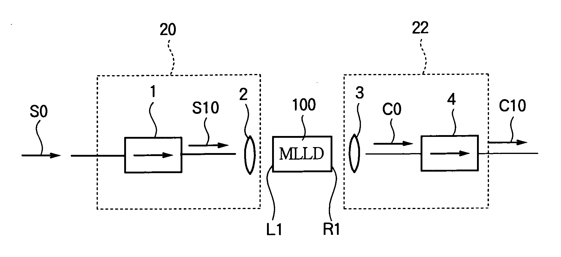
[0083]Referring to FIG. 1, the first embodiment is an optical clock signal recovery apparatus comprising a first polarization-dependent optical isolator 1 and a coupling lens 2 forming an optical input section 20, a coupling lens 3 and a second polarization-dependent optical isolator 4 forming an optical output section 22, and a mode-locked semiconductor laser, referred to below as a mode-locked laser diode (MLLD) 100, disposed between the optical input section 20 and the optical output section 22.

[0084]In the optical input section 20, the first polarization-dependent optical isolator 1 passes an input optical signal S0 received from an optical channel (not shown) through the coupling lens 2 to the mode-locked laser diode 100, and prevents light output from the mode-locked laser diode 100 from returning on the same optical channel. In the optical output section 22, the second polarization-dependent optical isolator 4 outputs the light generated by lasing in the mode-locked laser dio...

second embodiment

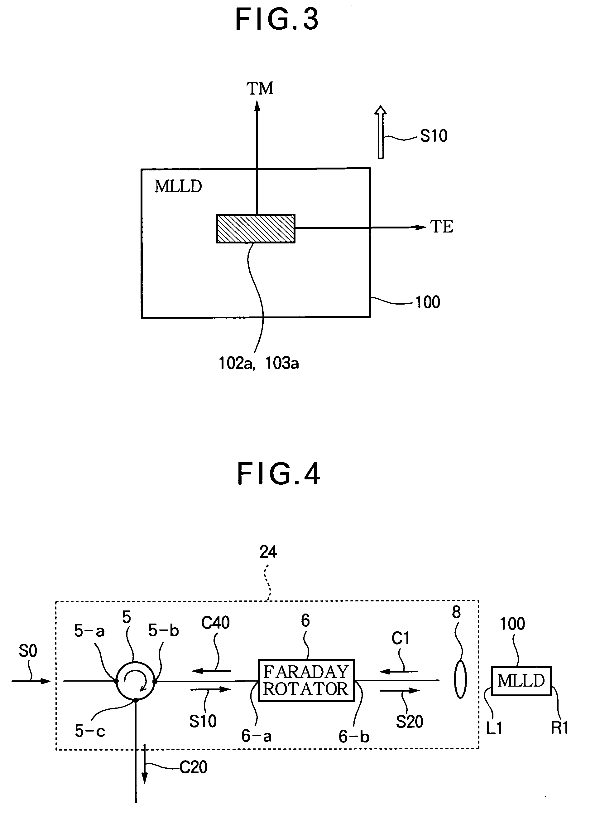
[0109]Referring to FIG. 4, in the second embodiment the input section and output section of the first embodiment are replaced by a single optical input-output section 24 disposed adjacent the left facet L1 of the mode-locked laser diode 100. The optical input-output section 24 comprises a polarization-dependent optical circulator 5, a Faraday rotator 6, and a coupling lens 8.

[0110]The polarization-dependent optical circulator 5 has an input port 5-a, an input-output port 5-b, and an output port 5-c. Light entering input port 5-a and polarized in a particular plane is output from input-output port 5-b. Light entering input port 5-a but polarized perpendicular to that plane is blocked. Similarly, light entering input-output port 5-b and polarized in the same particular plane is output from output port 5-c, while light entering input-output port 5-b but polarized perpendicular to that plane is blocked. A polarization-dependent optical circulator of this type can be constructed from pol...

third embodiment

[0115]Referring to FIG. 5, the third embodiment replaces the optical input-output section of the second embodiment with an optical input-output section 26 comprising a pair of polarization-dependent optical isolators 1, 4, a polarization-dependent optical coupler 7, and a coupling lens 9. The polarization-dependent optical isolators 1, 4 are similar to the polarization-dependent optical isolators in the first embodiment, the input optical signal S0 being input to the first polarization-dependent optical isolator 1 and the recovered optical clock signal C30 being output from the second polarization-dependent optical isolator 4.

[0116]The polarization-dependent optical coupler 7 has four ports 7-a, 7-b, 7-c, 7-d. Light input at port 7-a is coupled in equal or unequal portions to ports 7-b and 7-c. Light input at port 7-c is coupled in equal or unequal portions to ports 7-a and 7-d. The intensity ratio of the light output from port 7-b to the light output from port 7-c and the intensity...


PUM


Abstract

An optical clock signal recovery apparatus includes a mode-locked semiconductor laser that generates an optical pulse train polarized in a first direction. Optical components of the apparatus transmit a component of an input optical signal polarized in a second direction, perpendicular to the first direction, into the mode-locked semiconductor laser while blocking the component of the input optical signal polarized in the first direction, and transmit light exiting the mode-locked semiconductor laser polarized in the first direction, while blocking light exiting the mode-locked semiconductor laser polarized in the second direction. The transmitted exiting light is output as a recovered optical clock signal.

Description

BACKGROUND OF THE INVENTION[0001]1. Field of the Invention[0002]The present invention relates to an optical clock recovery apparatus and method useful in, for example, the optical repeaters of a long-haul fiber-optic communication system.[0003]2. Description of the Related Art[0004]Optical communication networks are transporting increasing quantities of data over increasing distances. With the increasing distances come increased problems of optical signal degradation, including waveform degradation in both the temporal and frequency domains. The causes are optical loss, signal-to-noise-ratio degradation owing to the use of multiple optical amplifier stages, and waveform distortion owing to group velocity dispersion. As transmission distances increase, these problems become increasingly apparent.[0005]For these reasons, repeaters are placed at intervals of a few tens of kilometers to a few hundred kilometers along the transmission route to regenerate optical signals by restoring thei...

Claims


Application Information

Patent Timeline
Patent Type & Authority Applications(United States)
IPC IPC(8): H04B10/00B82Y20/00H01S5/065H04B10/40H04B10/50H04B10/508H04B10/524H04B10/556H04B10/58H04B10/60
CPCH01S5/005H01S5/0064H01S5/0265H04L7/0075H01S5/0657H01S5/5036H01S5/0656
Inventor ARAHIRA, SHIN
Owner OKI ELECTRIC IND CO LTD
Why Eureka
Try Eureka