Protective layer setting unit, process cartridge, and image forming apparatus, and method of evaluating protective layer setting unit
a technology of protective layer and setting unit, which is applied in the direction of electrographic process apparatus, instruments, optics, etc., can solve the problems of short life of cleaning blade, reduced useful life of photoconductor, and ineffective capture of small toner particles by such a cleaning blad
- Summary
- Abstract
- Description
- Claims
- Application Information
AI Technical Summary
Benefits of technology
Problems solved by technology
Method used
Image
Examples
example 1-1
Methylene Index
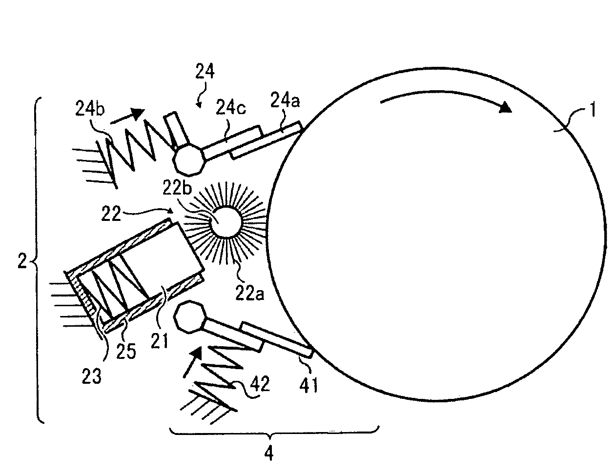
[0317]The photoconductor, a brush roller No.2 (fiber having a thickness of 10 denier, fiber density of 50,000 fibers per square inch), and a urethane blade were assembled in a protective layer setting unit (see FIG. 7). The agent bar No. 11 was pressed against the brush with a spring force of 4.8 N to apply a protective agent to photoconductors (1-1) to (1-5). The photoconductor and the brush roller rotated at a linear velocity of 125 mm / sec and 146 mm / sec, respectively.
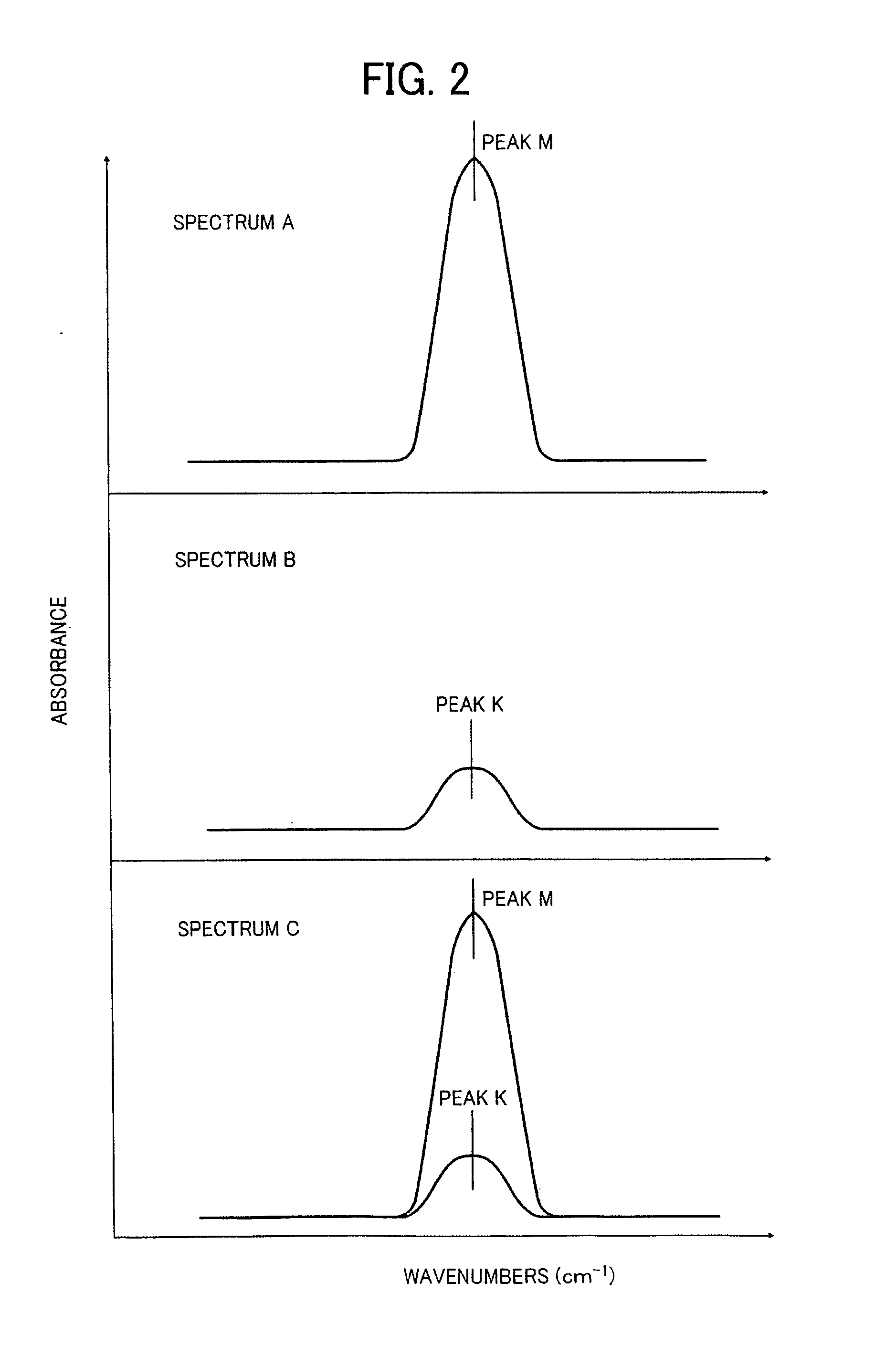
[0318]After applying the protective agent for 120 minutes to photoconductor (1-4) using the protective layer setting unit (11), a sample of the photoconductor was sliced using a ultramicrotome and TEM (transmission electron microscope) observation was conducted, and it was found that the layer thickness of protective agent was 20 nm to 50 nm based on TEM photo.
[0319]The photoconductors (1-1) to (1-5) were applied with the protective agent by changing an application time (3, 10, 40, 120, 360 minutes), a...
example 1-2
Phenyl Index
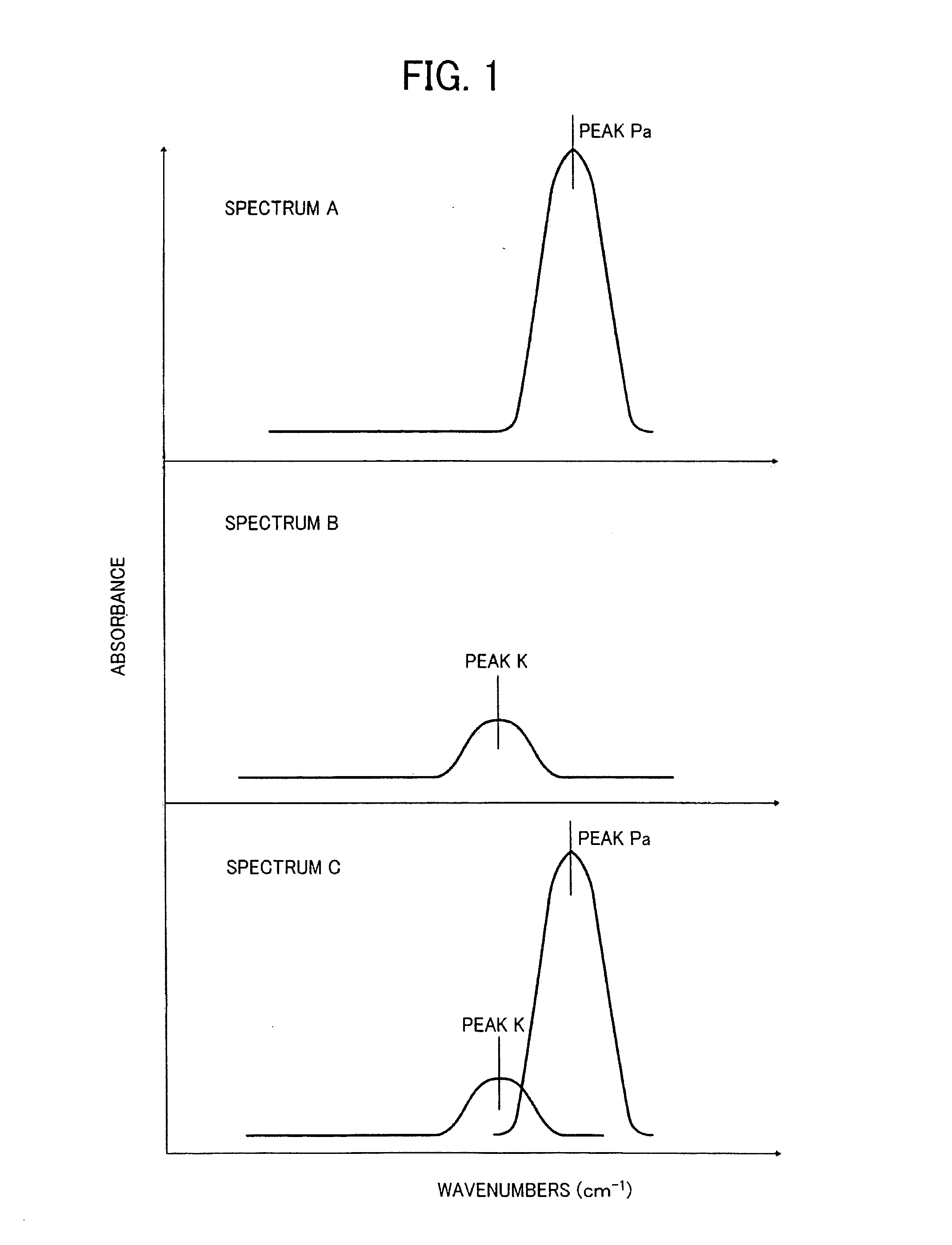
[0323]As for the IR spectrum obtained in Example 1-1, a peak area ratio or evaluation index “Sb / Sa” was computed for the peak Pb2 (2920 cm−1) having a peak area Sb and the peak Pa2 (3040 cm−1) having a peak area Sa. The peak Pb2 (2920 cm−1) is a peak attributed to the agent bar No. 11. Although a peak attributed to the photoconductor also exists around the peak Pb2 (2920 cm−1) and overlaps with the peak Pb2, the peak Pb2 (2920 cm−1) has a peak area sufficiently greater than the peak area of the peak attributed to the photoconductor. Accordingly, a step of computing a differential spectrum of the IR spectrum C after applying the protective agent to the photoconductor and the IR spectrum A for the photoconductor not applied with the protective agent was omitted, different from Example 1-1.
[0324]The evaluation index “Sb / Sa,” which indicates an application amount of the protective agent, increases as the application time increases. For example, the evaluation index “Sb / Sa” w...
example 1-3
[0325]The photoconductor, a brush roller No.3 (fiber having a thickness of 20 denier, fiber density of 50,000 fibers per square inch), and a urethane blade were assembled in a protective layer setting unit (see FIG. 7). The agent bar No. 11 was pressed against the brush with a spring force of 4.8 N to apply a protective agent to the photoconductors (3-1) to (3-5). The photoconductor and the brush roller rotated at a linear velocity of 125 mm / sec and 146 mm / sec, respectively.
[0326]The photoconductors (3-1) to (3-5) were applied with the protective agent by changing an application time (3, 10, 40, 120, 360 minutes), and samples of each the photoconductors were prepared after applying the protective agent. After applying the protective agent, samples of the photoconductors (3-1) to (3-5) were analyzed by FT-IR Avatar370 (manufactured by Thermo Electron Corporation, Thunder Dome) under a condition of one time reflection, ATR prism of Ge, incident angle of 45° for IR spectrum analysis to...
PUM
 Abstract
Description
Claims
Application Information


