
Thin-film materials, thin films and producing method thereof

a technology of thin film and material, applied in the field of thin film, can solve the problems of poor mechanical strength and thermal stability of film, film disruption, and insulating film formation according to this technique, and achieve the effects of low moisture absorption, low relative dielectric constant, and excellent mechanical strength

Inactive Publication Date: 2009-01-01
DAICEL CHEM IND LTD
View PDF2 Cites 7 Cited by
  • Summary
  • Abstract
  • Description
  • Claims
  • Application Information

AI Technical Summary

Benefits of technology

[0006]An object of the present invention is to provide: thin films, such as insulating films, which have high thermal stability and a low relative dielectric constant, are thereby useful for manufacturing of semiconductors, and have a pore structure with low moisture absorptivity; producing methods of these thin films; monomers and polymers capable of forming these thin films; and materials for film production, containing these monomers or polymers.

Problems solved by technology

This technique gives pores in the film, but inevitably causes binding of pores (connection or communication of pores), whereby the resulting film is inferior in mechanical strength and thermal stability.
This causes serious problems, such as film disruption, in interconnection processes of semiconductor manufacture.
Insulating films formed according to this technique, however, often have varying dielectric constants, because large amounts of unreacted terminals remain therein.

Method used


Image

  • Thin-film materials, thin films and producing method thereof
  • Thin-film materials, thin films and producing method thereof
  • Thin-film materials, thin films and producing method thereof

Examples


examples

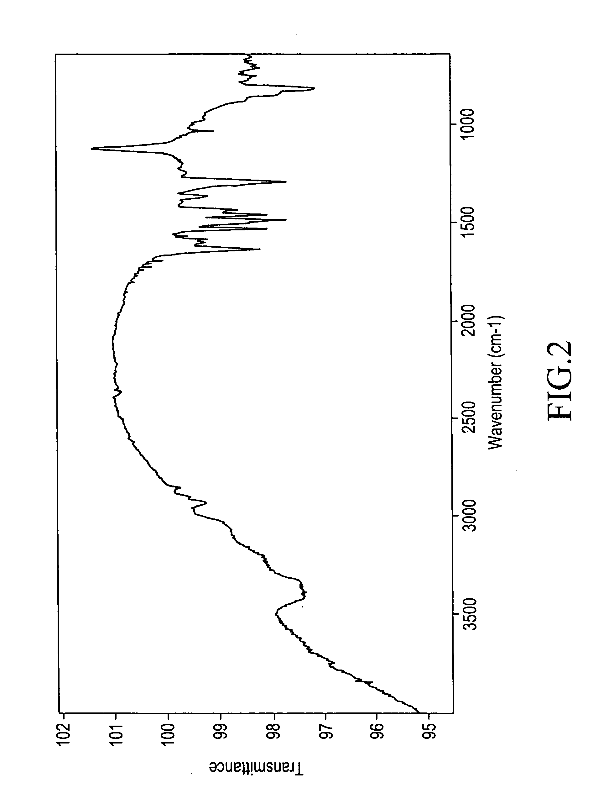
[0231]The present invention will be illustrated in further detail with reference to several examples below. It should be noted, however, these are never construed to limit the scope of the present invention. Thicknesses of polymer films were measured with an ellipsometer. Densities of the polymer films were determined by analysis of X-ray reflectance. Relative dielectric constants of the polymer films were measured in which an aluminum electrode was deposited on the surface of the films. Infrared absorption spectra were measured according to a thin-film transmission method. The symbols “s”, “m”, and “w” in the infrared absorption spectral data refer to “strong” absorption, “medium” absorption, and “weak” absorption. Weight-average molecular weights are in terms of polystyrene. Densities were measured at 25° C.

preparation example a1

[0232]Synthesis of Amino-Containing Adamantane Derivative of Formula (2-1):

[0233]In a reactor (three-necked flask) was placed 77.68 g (0.362 mol) of 3,3′-diaminobenzidine of Formula (2-4), and this was combined with 307 g of N,N-dimethylacetamide (DMAc), and dissolved to give a solution, and the solution was held at 0° C. or lower on an ice bath. To this solution was added dropwise, at a rate of 6 ml / min using a dropping funnel, another solution of 10.1 g (0.018 mol) of adamantane tetrakisbenzaldehyde of Formula (A) in 501 g of DMAC. The dropwise addition was conducted so that the temperature of the reaction mixture did not exceed 0° C. After the completion of dropwise addition, the dropping funnel was washed with 105 g of DMAc, and this washing was also added dropwise to the reaction mixture. While introducing a gaseous mixture of oxygen and nitrogen with an oxygen concentration of 5 percent by mole into the reaction mixture through a Teflon (registered trademark) tube, a reaction ...

preparation example a2

[0238]

[0239]In a 100-mL two-necked eggplant flask was placed 6 g (4.5 mmol) of the amino-containing adamantane derivative of Formula (2-1), and this was combined with 100 g of N,N-dimethylacetamide (DMAc), followed by stirring at room temperature in a nitrogen atmosphere for 10 minutes to give a solution. The solution was combined with 2.0 g (19 mmol) of benzaldehyde of Formula (D2) added dropwise, raised in temperature to 100° C., and stirred for 13 hours with air bubbling. The reaction mixture was added dropwise to 500 mL of water, filtrated, and thereby yielded 6.5 g of an adamantane derivative of Formula (E2) (terminally capped compound) as a solid in a yield of 86%.

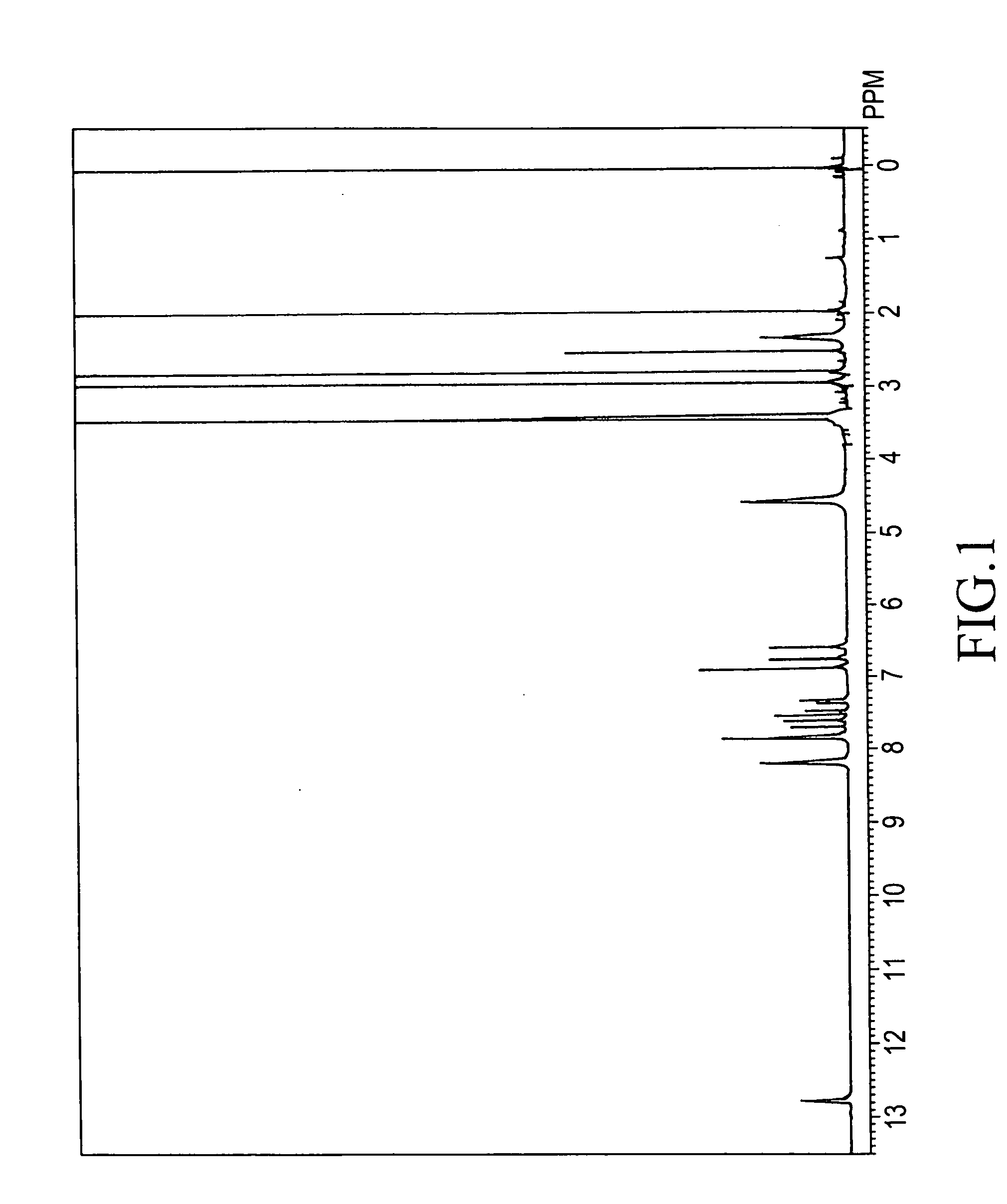
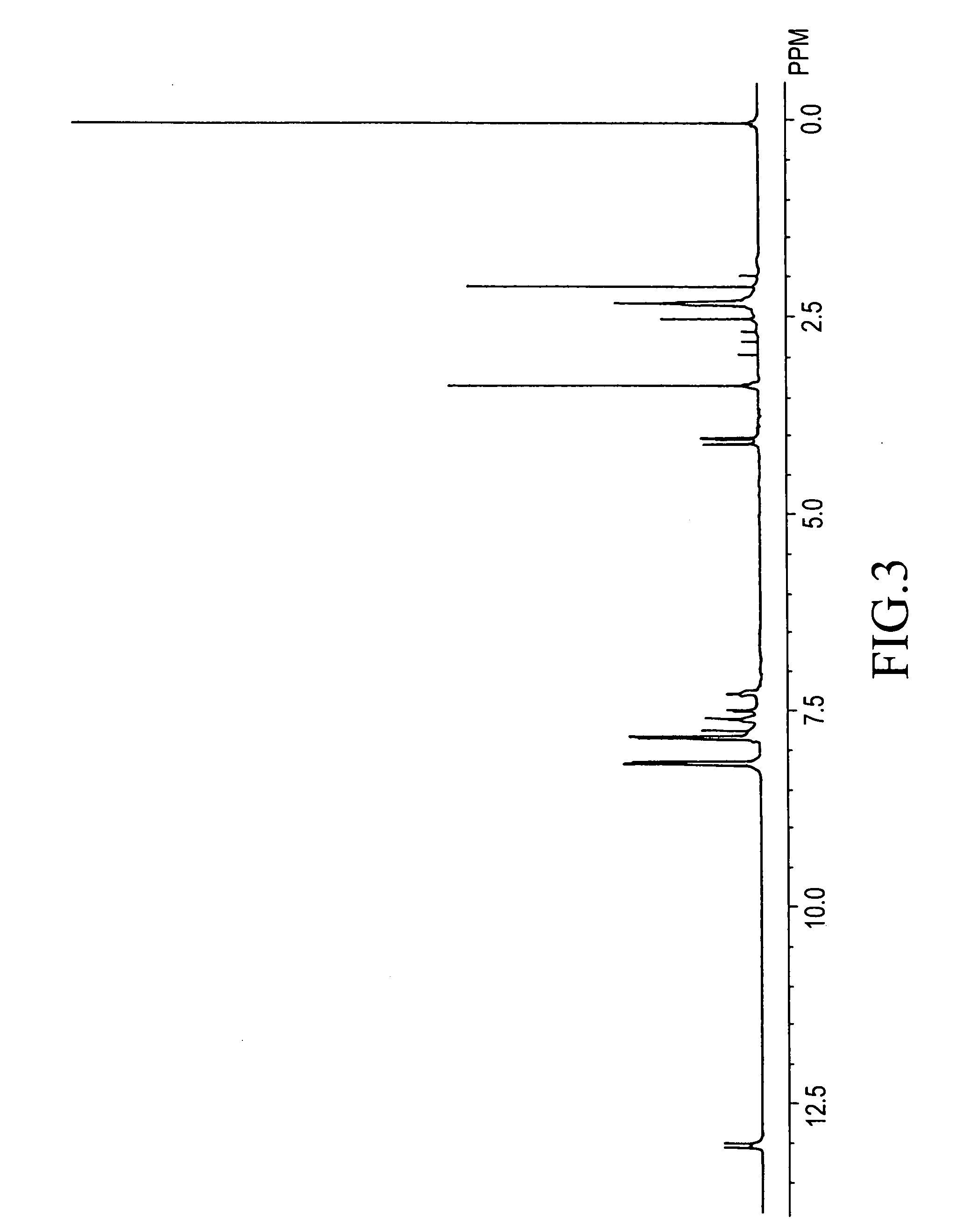
[0240][NMR Spectral Data]

[0241]1H-NMR (DMSO-d6) δ (ppm): 2.1-2.4 (12H), 7.4-8.4 (60H), 13.0 (8H)


PUM

PropertyMeasurementUnit
Molecular weightaaaaaaaaaa
Pore structureaaaaaaaaaa
aaaaaaaaaa

Abstract

An N-substituted benzimidazole-containing bridged alicyclic compound is provided. The compound is represented by following Formula (1-1):In the formula, Z3 represents a bridged alicyclic skeleton; Y11 represents a single bond or a divalent organic group; Y2 represents a single bond or a di- or tri-valent organic group; X3 represents a hydrogen atom or a reactive functional group; Ra represents a hydrogen atom or a hydrocarbon group; A3 represents a group represented by one of following Formulae (a) and (b):wherein R10 represents a monovalent organic group, wherein, in each of Formulae (a) and (b), the left side is to be bonded to Y11, and the right side is to be bonded to Y2; “n4” denotes an integer of 2 to 7; “m3” denotes an integer of 0 to 5; and “k2” denotes an integer of 0 to 2, wherein the total of “n4” and “m3” equals 2 to 7, and wherein two or more Y11s, Y2s, X3s, A3s, and R10s per molecule, and two or more X3s and Ras, if present per molecule, may be the same as or different from one another, respectively.

Description

BACKGROUND OF THE INVENTION[0001]1. Field of the Invention[0002]The present invention relates to thin films such as insulating films for use typically in manufacture of semiconductors, particularly to thin films such as insulating films that excel in thermal stability or mechanical strength or have low moisture absorptivity, and exhibit a low relative dielectric constant; producing methods of these thin films; monomers useful for the production of the insulating films; polymers obtained from the monomers; polymerizable compounds; and materials for forming thin films such as insulating films and polymers having a pore structure, which contain these.[0003]2. Description of the Related Art[0004]Finer circuit patterns in recent semiconductor processes require lower dielectric constants of interlayer dielectric films. It is believed that construction of a pore structure is effective to allow interlayer dielectric films to have a lower dielectric constant. Typically, there has been propos...

Claims


Application Information

Patent Timeline
IPC IPC(8): B32B9/00C08G73/06C07D235/04C07D498/04B05D3/02C07D497/00C08L39/00
CPCC07D235/18C07D235/20C08G61/123C08G73/18C08J5/18C08J2365/00H01L2924/12044C09D165/00C09D179/04H01B3/303H01L21/312H01L23/5329C08J2379/04H01L2924/0002H01L21/02203H01L21/02282H01L21/02118H01L2924/00C07D233/04C07D235/26C07D233/90C07D235/06
Inventor FUNAKI, YOSHINORIITAYA, RYOTAKARAGI, AKIRAOKAMOTO, KAZUKITORIEDA, MAYUMI
Owner DAICEL CHEM IND LTD
Learn More