Polycrystalline silicon substrate for magnetic recording media, and magnetic recording medium

a technology of polycrystalline silicon and recording media, applied in data recording, thin material processing, instruments, etc., can solve the problems of loss of recorded data, limited recording density growth, and serious heat fluctuation effect, and achieve low flying height and index dependence of polish rate.

Inactive Publication Date: 2009-01-15
SHIN ETSU CHEM IND CO LTD
View PDF11 Cites 6 Cited by
  • Summary
  • Abstract
  • Description
  • Claims
  • Application Information

AI Technical Summary

Benefits of technology

[0021]The present invention has been made in view of the foregoing problems. Accordingly, it is an object of the present invention to provide a polycrystalline Si substrate for magnetic recording media which has sufficient impact resistance and heat resistance, fails to complicate the fabrication process and the film formation process for a magnetic recording layer, exhibits such an excellent surface planarity as to allow a low flying height to be realized, and is inexpensive.
[0027]In the polycrystalline silicon substrate for magnetic recording media according to the present invention, the proportion of the {100} crystal faces, the polish rate of which is relatively high during crystal machining, and / or the proportion of the {111} crystal faces, the polish rate of which is relatively low during crystal machining, to the total area (S0) of the substrate surface is set to fall within an appropriate range. With this arrangement, the scale of “steps” formed due to the crystal face index dependence of polish rate can be reduced, which makes it possible to give a planar and smooth substrate surface.
[0028]As a result of planarization and smoothing of the substrate surface, a magnetic recording medium fabricated using such a substrate allows a low flying height to be realized. Also, the properties of polycrystalline Si as the material can assure that the substrate has sufficient impact resistance and heat resistance and fails to complicate the fabrication process and the film formation process for a magnetic recording layer. Further, the polycrystalline Si substrate can be utilized as an inexpensive polycrystalline Si substrate for magnetic recording media.

Problems solved by technology

As crystal grains are made more minute (i.e., reduced in volume) and recording bits made smaller in size, it is pointed out that a phenomenon called “heat fluctuation” occurs to disorder magnetization directions of crystal grains by thermal energy, thereby to cause a loss of recorded data.
Thus, the recording density growth has been considered to be limited.
The effect of the heat fluctuation becomes serious when the KuV / kBT ratio is too low.
HDD used in such a mobile application has a high possibility that its recording medium or substrate is damaged or data destroyed by “head-disk collision”.
Also, the downsizing of such a mobile device inevitably calls for downsizing and thinning of parts to be used therein.
Though a glass substrate having a diameter of 1 inch and a thickness of 0.382 mm has been put to practical use by mainly using reinforced amorphous glass, further thinning is not easy.
Further, since a glass substrate is an insulator, a problem arises that the substrate is likely to be charged up during formation of a magnetic film by sputtering.
Though volume production of such substrates is made practically possible by changing a holder holding a substrate to another one during sputtering, this problem is one of the factors that make the use of a glass substrate difficult.
Likewise, Al substrates cannot resist such a high temperature treatment.
However, the realities are such that any one of such substrates is inadequate for use as an alternative substrate for a small-diameter substrate in view of its strength, processability, cost, surface smoothness, affinity for film formation, and like properties.
However, Si single crystals of the “semiconductor grade” for fabrication of such devices as LSIs are generally expensive.
When consideration is given to the use of the single crystal Si substrate as a substrate for magnetic recording media, a serious problem arises that the single crystal Si substrate becomes inferior to glass substrates or Al substrates in terms of raw material cost as its diameter increases.
However, this measure gives rise to the following problem.
For this reason, it is difficult to obtain a smooth surface by CMP or the like.

Method used


Image

  • Polycrystalline silicon substrate for magnetic recording media, and magnetic recording medium
  • Polycrystalline silicon substrate for magnetic recording media, and magnetic recording medium
  • Polycrystalline silicon substrate for magnetic recording media, and magnetic recording medium

Examples


examples

[0067]Seven types of polycrystalline Si slugs were provided which were different in crystal purity and in contained impurity (i.e., dopant) from each other. Polycrystalline Si slugs of each type as raw material were put into a quartz glass crucible having a diameter of 180 mm provided in a melting furnace. With the crucible held at about 1,420° C. in an inert atmosphere, a melt of silicon was solidified at a rate of not less than 0.01 mm / min and less than 2 mm / min, to give a polycrystalline silicon ingot. Table 1 shows growth conditions for respective ingots as Examples 1 to 6 and Comparative Example 1.

TABLE 1Si purityResistanceSolidificationSamples(%)Impurity(Ω cm)rate (mm / min)Ex. 199.999B20.01Ex. 299.99P0.50.1Ex. 399.99Ge101Ex. 499.999B30.1Ex. 599.99B200.1Ex. 699.99B100.1Com.100B15Ex. 1

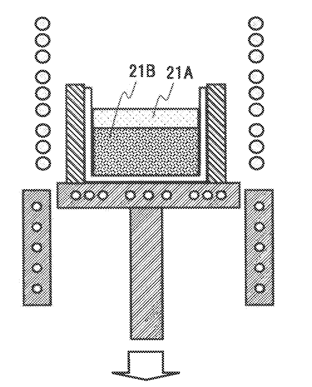
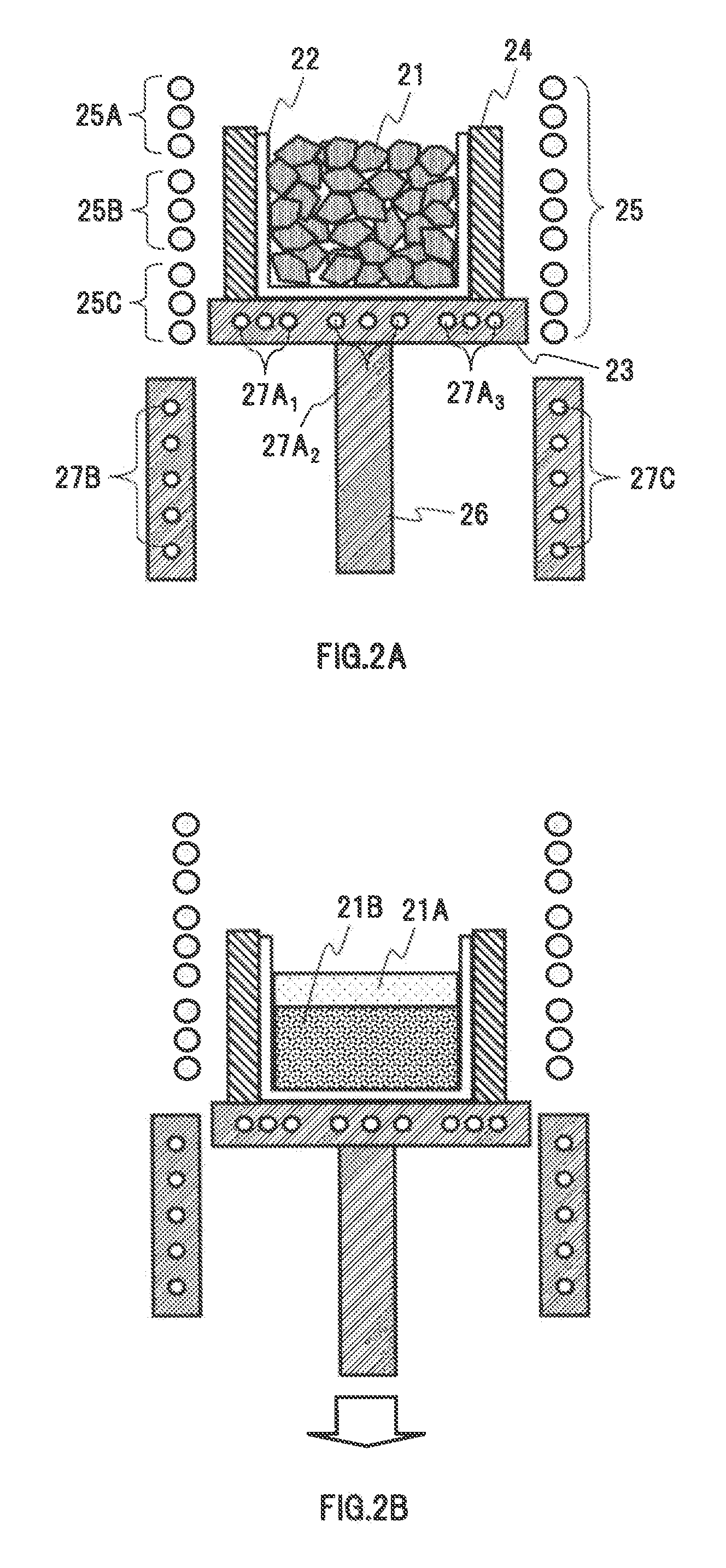
[0068]The polycrystalline silicon ingots thus obtained were each cut and lapped to give polycrystalline Si wafers (step S101). Thereafter, six polycrystalline Si substrates were obtained for each gr...


PUM

PropertyMeasurementUnit
thicknessaaaaaaaaaa
thicknessaaaaaaaaaa
thicknessaaaaaaaaaa

Abstract

The proportion of {100} crystal faces, the polish rate of which is relatively high during crystal machining, and / or the proportion of {111} crystal faces, the polish rate of which is relatively low during crystal machining, to the total area (S0) of a substrate surface, is set to fall within an appropriate range. Specifically, the proportion of the total area (S{100}) of the {100} crystal faces among crystal faces of individual crystal grains which appear on a major surface of a polycrystalline silicon substrate to the total area (S0) of the substrate surface, is set not less than 10% and less than 50%. Such crystal face selection makes it possible to reduce the scale of “steps” formed due to the crystal face index dependence of polish rate, thereby to give a planar and smooth substrate surface.

Description

BACKGROUND OF THE INVENTION[0001]1. Field of the Invention[0002]The present invention relates to a silicon substrate for use in fabricating a magnetic recording medium for hard disk drives and the like.[0003]2. Description of the Related Art[0004]In the technical field of information recording, a hard disk device as means for magnetically reading / writing such information as letters, images, or music is now indispensable as a primary external recording device or built-in type recording means for use with or in electronic devices including a personal computer. Such a hard disk device incorporates therein a hard disk as a magnetic recording medium. Conventional hard disks have employed a so-called “in-plane magnetic recording system (i.e., longitudinal magnetic recording system)” which writes magnetic information on a disk surface longitudinally.[0005]FIG. 1A is a schematic sectional view illustrating a typical stacked layer structure for a hard disk of the longitudinal magnetic record...

Claims


Application Information

Patent Timeline
Patent Type & Authority Applications(United States)
IPC IPC(8): G11B5/62
CPCY10T428/265G11B5/7315G11B5/73915Y10S428/90
Inventor TAKAI, YASUSHI
Owner SHIN ETSU CHEM IND CO LTD
Why Eureka
Try Eureka