Semiconductor nanocrystals for time domain optical imaging

a technology of time domain optical imaging and nanocrystals, applied in the field of optical imaging, can solve the problems of inability to determine the depth, inability to use visible light for most in vivo imaging applications, and inability to achieve depth, so as to increase the radiative decay rate, increase the pl dynamics, and reduce the effect of pl lifetim

Inactive Publication Date: 2009-01-22
NAT RES COUNCIL OF CANADA
View PDF2 Cites 8 Cited by
  • Summary
  • Abstract
  • Description
  • Claims
  • Application Information

AI Technical Summary

Benefits of technology

[0022]The semi-conductor nanocrystals of the invention can also be surface treated with inorganic materials and organic materials to increase the PL dynamics (namely to increase the radiative decay rate and thus to decrease PL lifetime) and to increase the population of short lifetime and decrease the population of long lifetime quantum dots.

Problems solved by technology

Such high tissue auto-fluorescence precludes the use of visible light for most in vivo imaging applications.
This intensity-based technology known as the continuous wave technique cannot discriminate photon absorption from photon scattering events, neither is it capable of determining the depth and concentration of the fluoroprobe.
However, conventional organic fluorophores suffer from significant limitations.
Organic fluorophores are difficult to tune to specific precise wavelengths due to the ‘inflexibility’ of their chemical structure.
The susceptibility of organic fluorophores to photobleaching limits the sensitivity of detection and often precludes repeated measurements.
However, there is little knowledge about the origin of the band-gap emission of semi-conductor nanocrystals, even with a cadmium selenide (CdSe) quantum dot, which is one of the most commonly studied systems.
Furthermore, there is lack of detailed studies on the photoluminescence lifetime.
(California) and Evident Technologies (New York) and NN-labs (Arkansas), have a long lifetime ranging between 20-400 nanoseconds, making them unsuitable for time-domain optical imaging applications which rely on a high repetition laser.

Method used


Image

  • Semiconductor nanocrystals for time domain optical imaging
  • Semiconductor nanocrystals for time domain optical imaging
  • Semiconductor nanocrystals for time domain optical imaging

Examples


Embodiment Construction

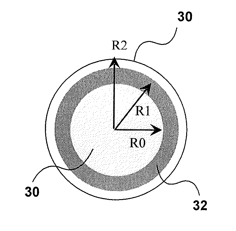
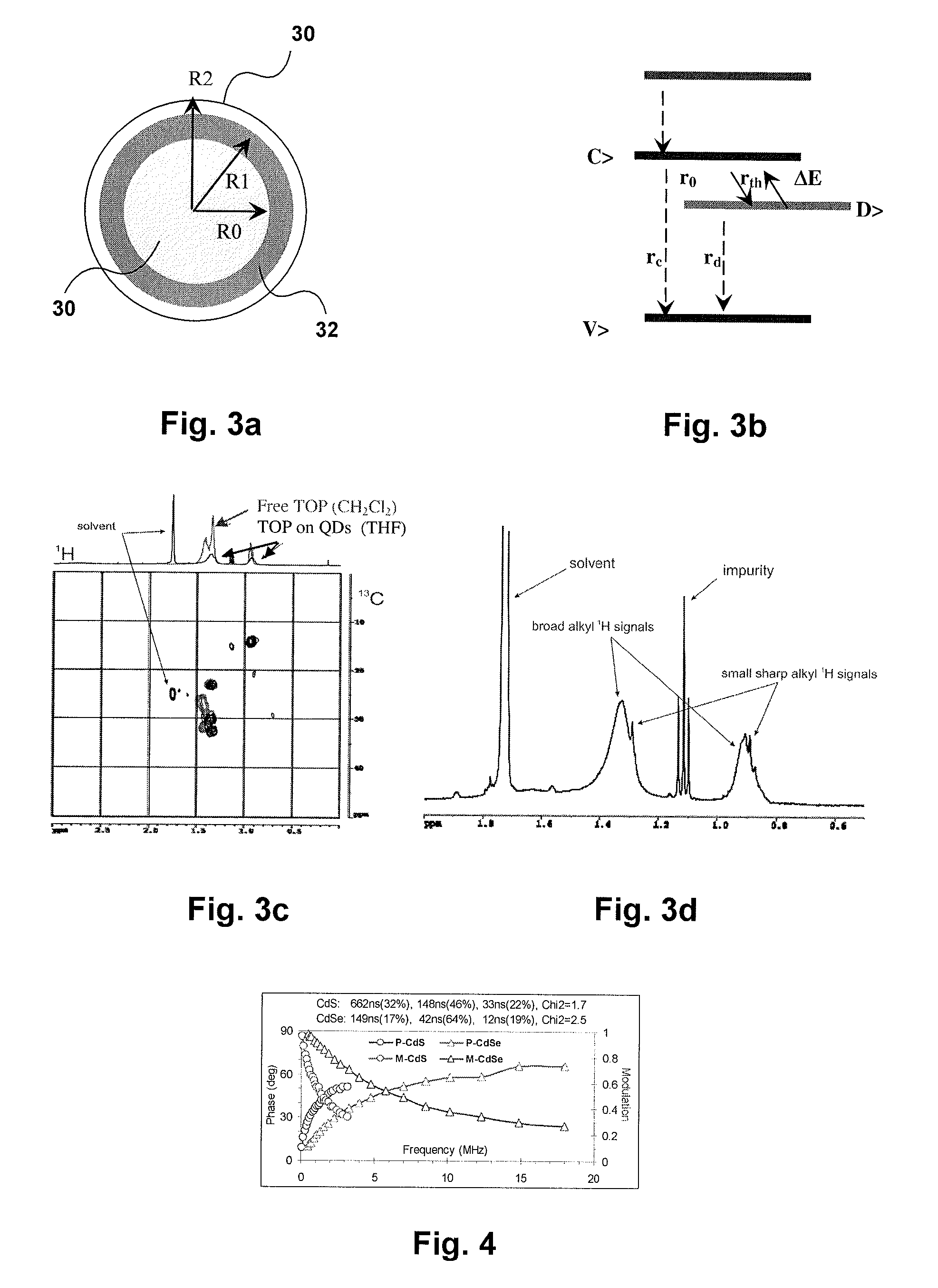
[0043]Various nanocrystallites were prepared as shown in FIG. 3a, which is a schematic model of one colloidal nano-crystallite which consists of three components, namely the capping ligand layer 30 which provides colloidal stability, the surface layer 32 between the core and the capping layer, and the core 30.

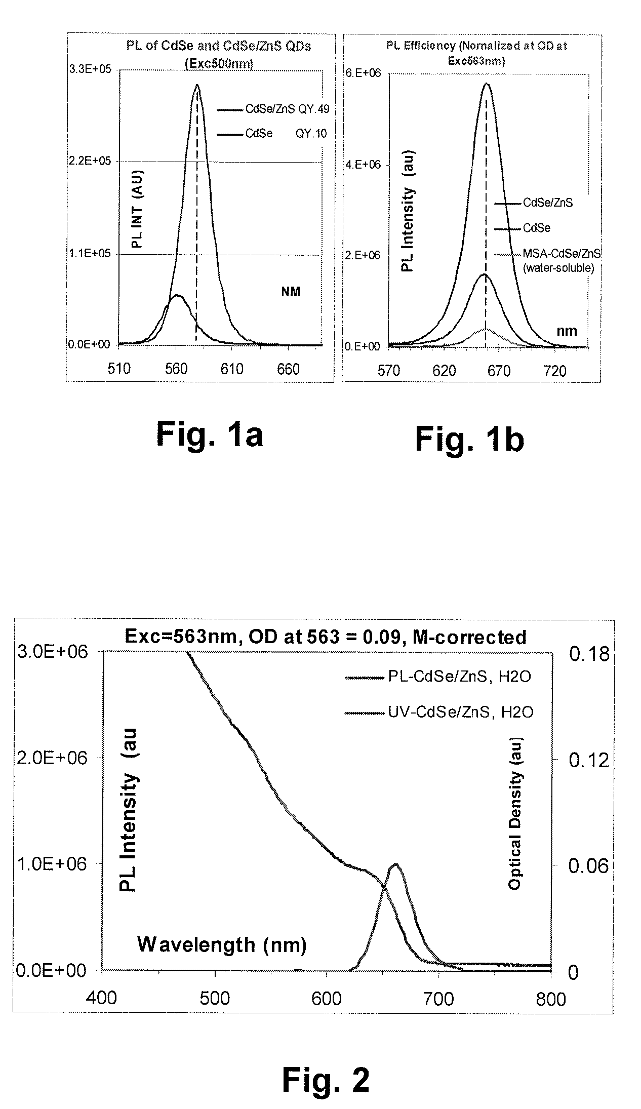
[0044]CdSe / ZnS core-shell quantum dots (QDs) were synthesized by sequential addition of a mixture of the Zn and S precursors into CdSe QDs in Tri-octylphosphine (TOP) (left) and TOP and amine (right). For the synthesis of CdSe QDs, CdO as the Cd source in the preparation of colloidal TOP-capped (left) and TOP-amine-capped (right) CdSe nano-crystals; the procedure involves nucleation at one temperature (250° C.-320° C.) followed by a period of growth at another temperature (250° C.-320° C.), without the use of any acid. Batches of CdSe nano-crystals were synthesized by which TOPSe / TOP solutions were injected into Cd-complex solutions in TOP or in a mixture of TOP and amine. The ...


PUM

PropertyMeasurementUnit
fluorescence lifetimeaaaaaaaaaa
temperaturesaaaaaaaaaa
emission wavelengthaaaaaaaaaa

Abstract

A method of performing high repetition rate laser time domain imaging employs as fluoroprobes semiconductor nanocrystals having a fluorescence lifetime less than the laser pulse separation, typically less than 5 ns. The nanocrystals of the invention have a core/shell structure and may be surface treated to increase radiative decay. CdSe/Zns nanocrystals are particularly suitable.

Description

FIELD OF THE INVENTION[0001]This invention relates to the field of optical imaging, and in particular time domain optical imaging technology that relies on high repetition rate lasers.BACKGROUND OF THE INVENTION[0002]Optical imaging technology for biomedical applications involves the analysis of photon propagation through tissues. An excitation photon typically travels through tissue to reach a fluorescent contrast agent, known as a fluorophore, and is affected by the scatter, anisotropy (g), and refractive index(ices) of the tissue. The photon emitted by the fluorophore is subject to the same factors. Due to the tissue absorbance, fluorescent light is also auto-emitted by the tissue. Such high tissue auto-fluorescence precludes the use of visible light for most in vivo imaging applications. The use of near infrared (NIR) light overcomes this problem by reducing the fluorescence background and thus optimizing the signal to background ratio (SBR).[0003]Traditional in vivo optical ima...

Claims


Application Information

Patent Timeline
Patent Type & Authority Applications(United States)
IPC IPC(8): G01J1/58H05B33/00C03B9/00
CPCA61K49/0067B82Y5/00C09K11/025C09K11/565G01N21/6489G01N21/6408G01N21/6428G01N21/6456C09K11/883
Inventor YU, KUIABULROB, ABEDELNASSER
Owner NAT RES COUNCIL OF CANADA
Why Eureka
Try Eureka