Chip for raman scattering enhancement and molecular sensing device including the chip

a molecular sensing and enhancement technology, applied in the field of chips for raman scattering enhancement and molecular sensing devices including chips, can solve the problems of lack of sensitivity for detecting specimens, raman activity, problem of detecting materials, etc., to suppress chemical reactions, detect molecules stably, and increase sensitivity

Inactive Publication Date: 2009-01-29
NAT INST OF ADVANCED IND SCI & TECH
View PDF6 Cites 18 Cited by
  • Summary
  • Abstract
  • Description
  • Claims
  • Application Information

AI Technical Summary

Benefits of technology

[0013]According to the present invention, it can detect molecules with higher sensitivity than the conventional molecular sensing device using the thin film containing the noble metal oxide (or noble metal oxide film). In addition, it can suppress a chemical reaction between the noble metal oxide and the molecules to be detected or a solution or gas containing the molecules to be detected, and can detect the molecules stably and at higher accuracy.

Problems solved by technology

The molecular sensor, which uses silver particles formed by decomposition of a silver oxide by laser beam irradiation or the like, has a drawback of being lacking of sensitivity for detecting a specimen (such as molecules) with low Raman activity.
In addition, a metal oxide like a silver oxide is high oxidative, and oxidizes the specimen or a solvent including the specimen, there by changing the quality thereof.
As a result, it has a problem of detecting a material not included in the solvent originally.

Method used


Image

  • Chip for raman scattering enhancement and molecular sensing device including the chip
  • Chip for raman scattering enhancement and molecular sensing device including the chip
  • Chip for raman scattering enhancement and molecular sensing device including the chip

Examples


example 1

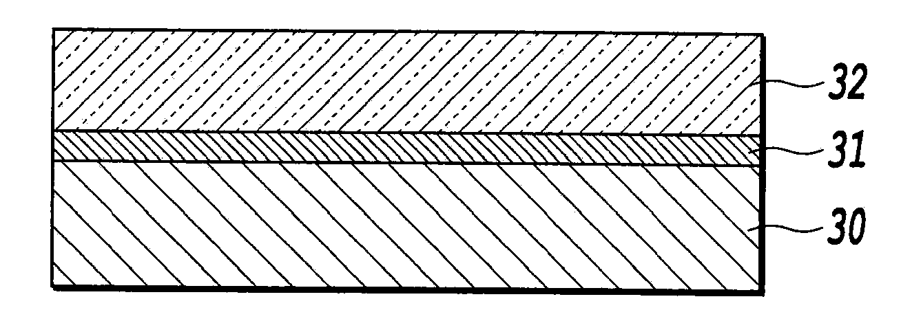
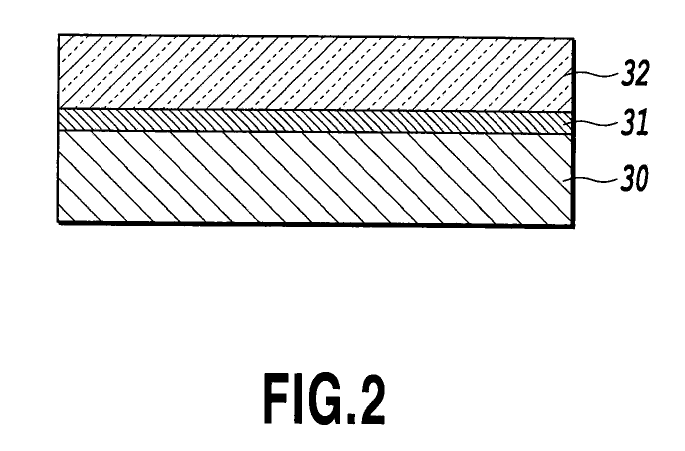
[0092]The present example shows a case where the layer containing the noble metal oxide is formed on the substrate, and the dielectric material thin film layer is further formed thereon. For comparison purposes, results are also shown when using a chip (comparative chip A) without the dielectric material thin film layer, and a chip (comparative chip B) with only the substrate.

[0093]As the substrate, a silicon substrate 1 cm square and 525 μm thick was used. As the layer containing the noble metal oxide, a silver oxide was used. The silver oxide was formed by the reactive sputtering method that set Ag as a target and used a gas mixture of oxygen and Ar as a reactive gas. In that case, the flow ratio O2 / (Ar+O2) between the oxygen and Ar was set at 0.75. The composition of the silver oxide formed includes Ag and O at a ratio of one to one, which means that it is AgO. Thus, the silver oxide thin film is referred to as an AgO thin film from now on. In addition, sputtering was carried out...

example 2

[0100]By the same silver oxide thin film formative method as that of the example 1, an AgO thin film with a film thickness of 15 nm was formed on a silicon substrate. Then, five silicon oxide film layers with different film thicknesses of 40 nm, 80 nm, 160 nm, 320 nm and 640 nm were formed thereon to fabricate five chips. The silicon oxide film formative method was the same as that of the example 1. Besides, as a comparative chip, a chip was prepared which had the same AgO thin film but did not have the silicon oxide film layer.

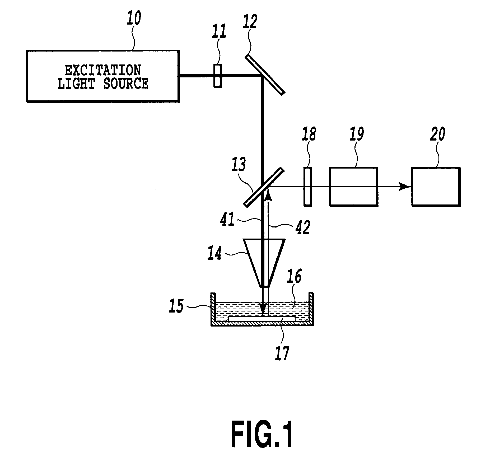
[0101]As the specimen, a solution was used which dissolved BA in a solvent IPA by 1.0×10⁻⁵ mol / l, and the Raman scattering measurement was carried out in the same configuration as that of FIG. 7(a) as in the example 1. The present example employed a He—Ne laser (wavelength 633 nm) as the light source for the Raman scattering measurement. In this case also, the formation of the particles containing silver was performed using the light source for the Raman scat...

example 3

[0105]By the same method as that of the example 1, the present example fabricated two types of chips for Raman scattering enhancement having the AgO thin film with a film thickness of 15 nm or 50 nm, and the Raman scattering measurement was performed for a solution that dissolved BA in a solvent IPA by 1.0×10⁻⁵ mol / l in the configuration of FIG. 7(a) as in the example 1. In the present example, an Ar ion laser (wavelength 488 nm and intensity 2.7 mW) was used as the light source for the Raman scattering measurement. The film thickness of the dielectric layer (silicon oxide film layer) of the chip for Raman scattering enhancement was made 80 nm. As for the formative method of the silicon oxide film and the formation of the particles containing silver, they were the same as those of the example 1.

[0106]As a result, as for the chip for Raman scattering enhancement having the AgO thin film with the film thickness of 15 nm, the peak intensity at 1002 cm−1 due to BA after five minutes ela...


PUM


Abstract

The present invention aims to provide a chip applied to a molecular sensing device which carries out Raman spectroscopic analysis utilizing Raman scattering enhancement due to plasmons, and that achieves higher sensitivity and stability of its sensing sensitivity and miniaturization, and to provide a molecular sensing device including the chip. As the chip for Raman scattering enhancement applied to the molecular sensing device using the Raman spectroscopic analysis, which has an excitation light source for Raman scattering, a chip for Raman scattering enhancement and a photodetector for observing the Raman scattering, the present invention employs a chip having a molecular detecting element in which a transparent protection material thin film 32 composed of a dielectric material thin film or semiconducting material thin film is formed on a thin film 31 containing the noble metal oxide, and utilizes the Raman scattering enhancement by the thin film containing the noble metal oxide.

Description

TECHNICAL FIELD[0001]The present invention relates to a chip for Raman scattering enhancement, which is used as a sensor of a molecular sensing device (molecular sensor) for sensing molecules by Raman spectroscopic analysis, and a molecular sensing device including the chip.BACKGROUND ART[0002]Enhancement of Raman scattered light (Raman scattering enhancement) using plasmons generated on a metal thin film surface or metal particle surface is know as surface enhanced Raman scattering (SERS), and applications to detection and identification of various materials have been reported. For example, J. Appl. Phys., Vol. 88, No. 11, pp. 6187-6191 (2000) describes Raman spectroscopic analysis utilizing electric field enhancement by surface plasmon-polariton. In this paper, Raman spectroscopic analysis of a TiO2 thin film existed on an Ag thin film is carried out using the surface plasmon resonance of the silver thin film formed on a glass substrate. Such Raman scattering enhancement using the...

Claims


Application Information

Patent Timeline
Patent Type & Authority Applications(United States)
IPC IPC(8): G01J3/44
CPCG01N21/65G01N2021/651G01N21/658
Inventor FUJIMAKI, MAKOTOTOMINAGA, JUNJIIWANABE, YASUHIKO
Owner NAT INST OF ADVANCED IND SCI & TECH
Why Eureka
Try Eureka