Thin-Film Solid Secondary Cell

a thin film solid and secondary cell technology, applied in the field of thin film solid secondary cells, can solve the problems of inadequacies in advancing a further reduction in thickness or size, affecting the production efficiency of final products, and requiring formation time and formation cost, etc., to achieve excellent cell characteristics, stably created, and the effect of increasing the charge/discharge capacity

Inactive Publication Date: 2009-01-29
GEOMATEC
View PDF10 Cites 32 Cited by
  • Summary
  • Abstract
  • Description
  • Claims
  • Application Information

AI Technical Summary

Benefits of technology

[0032]According to the present invention, since at least the layers (the positive electrode active material layer, the solid electrolyte layer, and the negative electrode active material layer) other than the collector layers in the constituent thin films are amorphous, a stress is small, and film exfoliation hardly occurs even if the entire film thickness is increased to heighten the charge / discharge capacity. Additionally, since a material containing lithium is used for the positive electrode active material layer, lithium does not have to be injected on a later stage, and the thin-film solid secondary cell having excellent cell characteristics can be stably created with reduced manufacturing time and steps. Further, the cell characteristics, e.g., an increase in the charge / discharge capacity, stabilization of cycle characteristics, or a reduction in a speed of a voltage drop can be improved by specifying materials used for the positive electrode active material layer and the negative electrode active material layer. Furthermore, since a vanadium oxide is not used for the negative electrode active material layer, an influence of moisture is not given, and poisonous properties do not become a problem, and processing can be facilitated.

Problems solved by technology

However, in recent years, a polymer cell using a gel electrolyte, not an electrolytic solution (see, e.g., Patent Document 1) or a thin-film solid secondary cell (see, e.g., Patent Documents 2 to 4) using a solid electrolyte has been developed to enable a further reduction in thickness and size.
Such a polymer cell can be reduced in thickness and size as compared with a regular lithium-ion secondary cell using an electrolytic solution, but its thickness is limited to approximately 0.1 mm because it requires a gel electrolyte, a bond, an opening sealing member, and others, and hence it is not appropriate to advance a further reduction in thickness or size.
When lithium is injected into the negative electrode side in this manner, since a negative electrode layer must be once taken out into the atmosphere after the negative layer is formed and lithium must be injected into this layer by using a lithium injection device, the injection device is required and an injecting operation takes time, and hence there is a problem that a formation time and a formation cost are additionally required.
Further, the negative electrode layer made of, e.g., a vanadium oxide with lithium injected therein is apt to be oxidized, and weak in moisture.
Therefore, degradation in properties of film, e.g., oxidation or moisture absorbent is often-caused when injecting lithium, and there is a problem that the thin-film solid secondary cell with excellent cell characteristics cannot be stably formed.
Furthermore, there is also a problem that processing a vanadium oxide is troublesome in a manufacturing process or during use of a cell since this material has poisonous properties.
However, when a vanadium oxide is used for the negative electrode layer, there is a problem that a voltage is rapidly reduced at the time of discharge and a capacity which can maintain a voltage equal to or above approximately 1 V required for driving a regular device is small as compared with a usual solution type secondary cell.
Additionally, as explained above, there is a problem that the vanadium oxide is weak in moisture and processing this oxide is trouble since it has poisonous properties.
As explained above, the vanadium oxide used as the negative electrode material has a problem in processing and cell characteristics.
However, when a lithium phosphate which is stable and has relatively high ion-conducting properties is used for the solid electrolyte layer, a reaction occurs on an interface between any other negative electrode material and the lithium phosphate and another product is formed, and hence a problem of degradation in cell characteristics occurs.

Method used


Image

  • Thin-Film Solid Secondary Cell
  • Thin-Film Solid Secondary Cell
  • Thin-Film Solid Secondary Cell

Examples


example 1

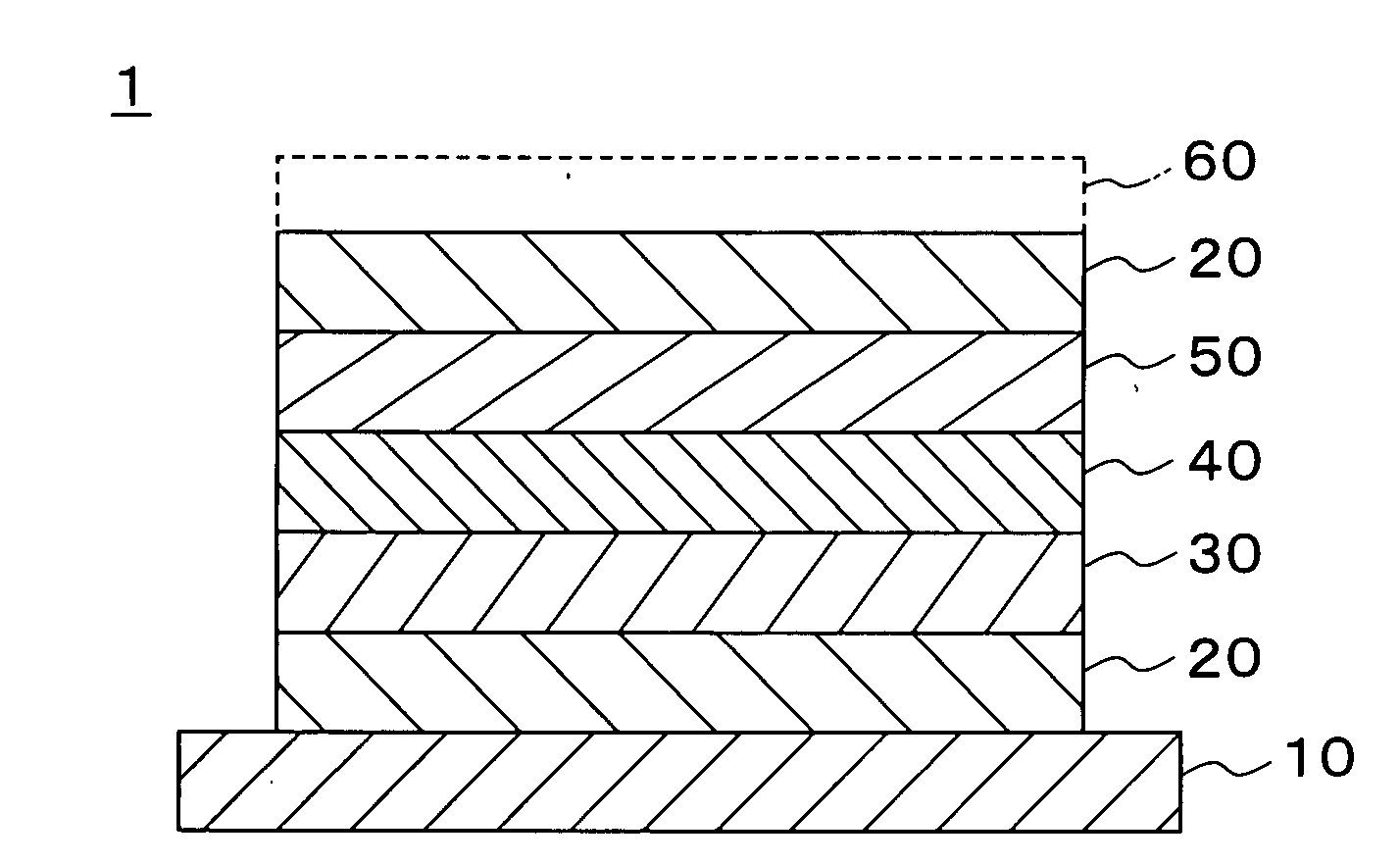
[0056]In Example 1, a collector layer 20, a positive electrode active material layer 30, a solid electrolyte layer 40, a negative electrode active material layer 50, and the collector layer 20 were formed on a substrate 10 in this order by a sputtering method to provide a structure depicted in FIG. 1, thereby creating a thin-film solid secondary cell.

[0057]Soda lime glass having a vertical dimension of 100 mm, a lateral dimension of 100 mm, and a thickness of 1 mm was used for the substrate 10.

[0058]The collector layer 20 was formed by a DC magnetron sputtering method using a vanadium metal target. A DC power was 1 KW, and the film was formed without heating. As a result, a vanadium thin film of 0.3 μm was formed as the collector layer 20.

[0059]The positive electrode active material layer 30 was formed by an RF magnetron sputtering method using a sintered body target of a lithium manganate (LiMn2O4) and introducing oxygen. An RF power was 1 KW, and the film was formed without heatin...

example 2

[0068]In Example 2, a thin-film solid secondary cell having the structure depicted in FIG. 1 was created by a sputtering method. Layers other than a negative electrode active material layer 50 were formed with the same materials, the same film thicknesses, and the same film forming conditions as those in Example 1. The negative electrode active material layer 50 was formed by a DC magnetron sputtering method using an S—Mn alloy target at %). A DC power was 1 KW, and the film was formed without heating. As a result, an S—Mn alloy thin film of 0.3 μm was formed as the negative electrode active material layer 20.

[0069]In the following examples and comparative example, the same X-ray diffraction measurement as that in Example 1 was carried out, and the charge / discharge characteristics were measured under the same measurement conditions unless stated.

[0070]A diffraction peak did not appear in the X-ray diffraction measurement, and it was confirmed that all the constituent layers in the t...

example 3

[0077]In Example 3, a thin-film solid secondary cell having the structure depicted in FIG. 1 was created by a sputtering method. Layers other than a negative electrode active material layer 50 were formed with the same materials, the same film thicknesses, and the same film forming conditions as those in Example 1. The negative electrode active material layer 50 was formed by an RF magnetron sputtering method using a sintered body target of an indium oxide having tin added therein (ITO) and introducing oxygen. An RF power was 1 KW, and the film was formed without heating. As a result, an ITO thin film of 0.3 μm was formed.

[0078]A diffraction peak did not appear in the X-ray diffraction measurement, and it was confirmed that all the constituent layers in the thin-film solid secondary cell are amorphous.

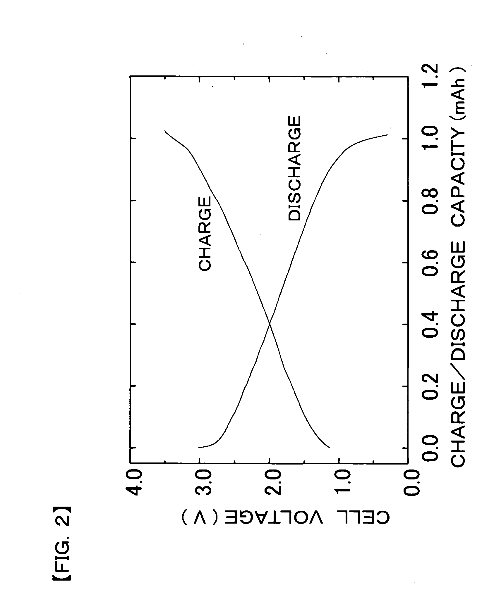
[0079]In the measurement of the charge / discharge characteristics, it was confirmed that the thin-film solid secondary cell repeatedly demonstrates a charge / discharge operation. FIG. 4 ...


PUM

PropertyMeasurementUnit
electrode potentialaaaaaaaaaa
volumeaaaaaaaaaa
thicknessaaaaaaaaaa

Abstract

Disclosed is a thin-film solid secondary cell (1) wherein a positive electrode collector layer (20), a positive electrode active material layer (30), a solid electrolyte layer (40), a negative electrode active material layer (50) and a negative electrode collector layer (20) are arranged on a substrate (10). The positive electrode active material layer (30) is a thin film composed of a metal oxide containing a transition metal and lithium, while the negative electrode active material layer (50) is a thin film composed of a semiconductor, a metal, an alloy or a metal oxide other than vanadium oxide. At least layers other than collector layers (20) are amorphous thin films. The substance constituting the solid electrolyte layer (40) is lithium phosphate (Li3PO4) or lithium phosphate added with nitrogen (LIPON).

Description

TECHNICAL FIELD[0001]The present invention relates to a thin-film solid secondary cell, and more particularly to a thin-film solid secondary cell which can be reduced in thickness and size.BACKGROUND ART[0002]At the present day, a lithium-ion secondary cell is extensively used mainly in electronic devices, e.g., a portable device. That is because the lithium-ion secondary cell has a high voltage and high charge / discharge capacity but does not have a problem in a memory effect as compared with a nickel-cadmium cell and others.[0003]Further, a further reduction in size / weight has been advanced in electronic devices and others, and development for a reduction in size / weight has also been promoted in the lithium-ion secondary cell as a battery which is mounted on the electronic devices and others. For example, a lithium-ion secondary cell which can be mounted in an IC card, a medical small device, and others and reduced in thickness / size has been developed. Furthermore, demanding a furt...

Claims


Application Information

Patent Timeline
Patent Type & Authority Applications(United States)
IPC IPC(8): H01M6/18H01M4/131H01M4/134H01M4/136H01M4/48H01M4/485H01M4/50H01M4/505H01M4/52H01M4/525H01M4/58H01M10/0525H01M10/0562H01M10/0585H01M10/36
CPCH01M4/131H01M4/134H01M4/136H01M4/40H01M4/405H01M4/485Y02E60/122H01M4/525H01M4/5825H01M10/0525H01M10/0562H01M10/0585H01M4/505H01M4/38H01M4/386Y02E60/10Y02P70/50
Inventor NAKAZAWA, HIROMISANO, KIMIHIROBABA, MAMORU
Owner GEOMATEC
Why Eureka
Try Eureka