Organic electroluminescent element

a technology of electroluminescent elements and organic materials, applied in the direction of discharge tubes/lamp details, discharge tubes luminescnet screens, other domestic articles, etc., can solve the problems of reducing the light emitting efficiency, reducing the current density, and reducing the light transmittance efficiency, so as to improve the electrical conductivity of the semiconductor buffer layer or the semiconductor electrode layer, the effect of reducing the light transmittan

Inactive Publication Date: 2009-02-26
DAI NIPPON PRINTING CO LTD +1
View PDF20 Cites 8 Cited by
  • Summary
  • Abstract
  • Description
  • Claims
  • Application Information

AI Technical Summary

Benefits of technology

[0023]Further, in the present invention, it is preferable that the semiconductor buffer layer or the semiconductor electrode layer has a thickness in a range of 1 nm to 500 nm, and an average light transmittance in a visible region is 30% or more. This is because there is a possibility that the light transmittance is lowered when the thickness of the semiconductor buffer layer or the semiconductor electrode layer is too thick. Conversely, when the thickness of the semiconductor buffer layer is too thin, there is a possibility that effect of protecting the organic EL layer from impact, at formation of the second electrode layer, is not obtained. And also, when the thickness of the semiconductor electrode layer is too thin, there is a possibility that the layer does not perform a function as an electrode.
[0024]In addition, in the present invention, it is preferable that a content of the metal in the semiconductor buffer layer or the semiconductor electrode layer is in a range of 0.0001% by volume to 90% by volume. When the content of the metal is too much, there is a possibility that the light transmittance of the semiconductor buffer layer or the semiconductor electrode layer is lowered. Conversely, when the content of the metal is too little, there is a possibility that effect of enhancing electrical conductivity of the semiconductor buffer layer or the semiconductor electrode layer is not obtained.
[0025]Further, in the present invention, it is preferable that, the metal is contained in the semiconductor buffer layer or the semiconductor electrode layer so that, when a metal contained in the semiconductor buffer layer or the semiconductor electrode layer is formed into a layer consisting only of the metal, a thickness of the layer consisting only of the metal is 100 nm or less. When the thickness of the layer consisting only of the metal is too thick, there is a possibility that the light transmittance of the semiconductor buffer layer or the semiconductor electrode layer is reduced.
[0026]In addition, in the present invention, it is preferable the semiconductor buffer layer or the semiconductor electrode layer is formed into a film by a vacuum deposition method. In the vacuum deposition method, since oxygen is not usually introduced, for example, even when the electron injecting layer is formed between the light emitting layer and the semiconductor buffer layer or the semiconductor electrode layer, oxidation of the metal contained in this electron injecting layer can be avoided.
[0027]Further, in the present invention, a charge injecting / transporting layer may be formed between the light emitting layer, and the semiconductor buffer layer or the semiconductor electrode layer. This is because this can stabilize injection of a charge into the light emitting layer, and enhance the light emitting efficiency.
[0028]In the present invention, since the semiconductor buffer layer is formed between the organic EL layer and the second electrode layer, damage of the organic EL layer due to impact at formation of the second electrode layer can be alleviated. In addition, for example, even when the electron injecting layer is formed between the light emitting layer and the semiconductor buffer layer, oxidation of the metal contained in this electron injecting layer can be prevented. As described above, in the present invention, such effect can be exerted that property deterioration of the organic EL layer and light emitting property deterioration of the organic EL element can be suppressed.

Problems solved by technology

And there arises a problem that, upon formation of the transparent electrode, the organic EL layer containing the light emitting layer, and the electron injecting layer or the hole injecting layer are shocked by sputtered particles, Ar+ at sputtering, and an ionized electron, so that the light emitting property is deteriorated (reduction in current density, reduction in light emitting efficiency, leakage of current).
Further, there is also a problem that, upon formation of the transparent electrode as the cathode, a highly reactive metal contained in the electron injecting layer is oxidized due to oxygen introduction or release of oxygen from a target, and deterioration in property of the organic EL layer and the electron injecting layer (reduction in current density property, reduction in light emitting efficiency, increase in dark spot) is caused.
When there are these problems, a high quality image display cannot be obtained.
However, when the aforementioned buffer layer or barrier layer (organic substance, semiconductor etc.) is inserted, in particular, in an organic EL element which is driven under a high current density (organic EL element using a conductive polymer), there is a problem that current density-voltage property is deteriorated as compared with the conventional organic EL element which takes emitted light out from the bottom side.

Method used


Image

  • Organic electroluminescent element
  • Organic electroluminescent element
  • Organic electroluminescent element

Examples


first embodiment

1. FIRST EMBODIMENT

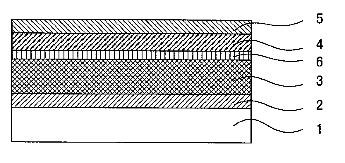
[0039]The first embodiment of the organic EL element of the present invention is characterized in comprising: a substrate; a first electrode layer formed on the substrate; an organic electroluminescent layer which is formed on the first electrode layer, and has at least a light emitting layer; a semiconductor buffer layer which is formed on the organic electroluminescent layer, and contains an inorganic compound having a band gap of 2.0 eV or more and a metal; and a second electrode layer formed on the semiconductor buffer layer.

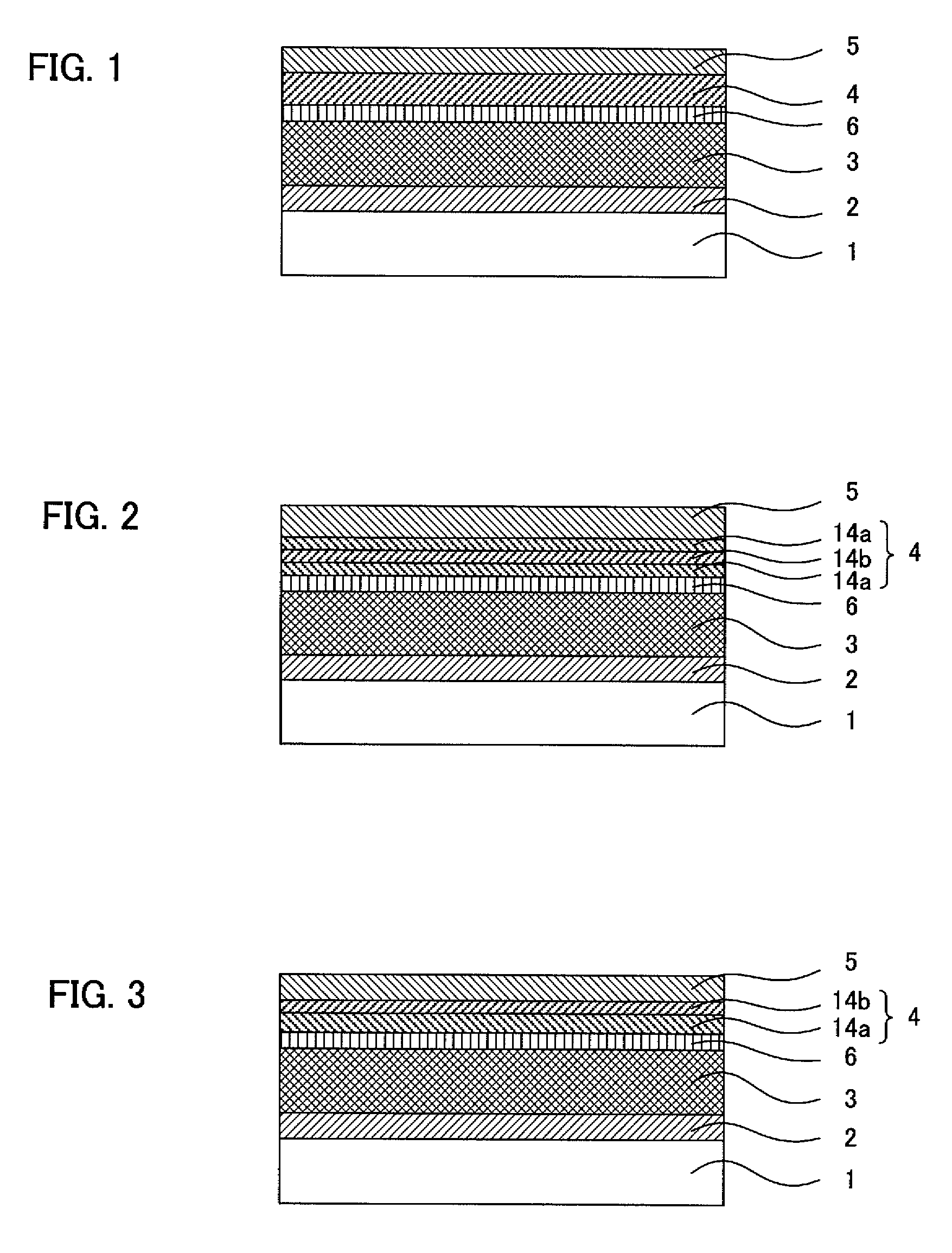
[0040]The organic EL element of the present embodiment will be explained by referring to the drawings. FIG. 1 is a schematic cross-sectional view showing one example of the organic EL element of the present embodiment. In FIG. 1, an organic EL element comprises: a substrate 1; a first electrode layer 2 formed on the substrate 1; an organic EL layer 3 which is formed on the first electrode layer 2 and has at least a light emitting layer; an...

second embodiment

2. SECOND EMBODIMENT

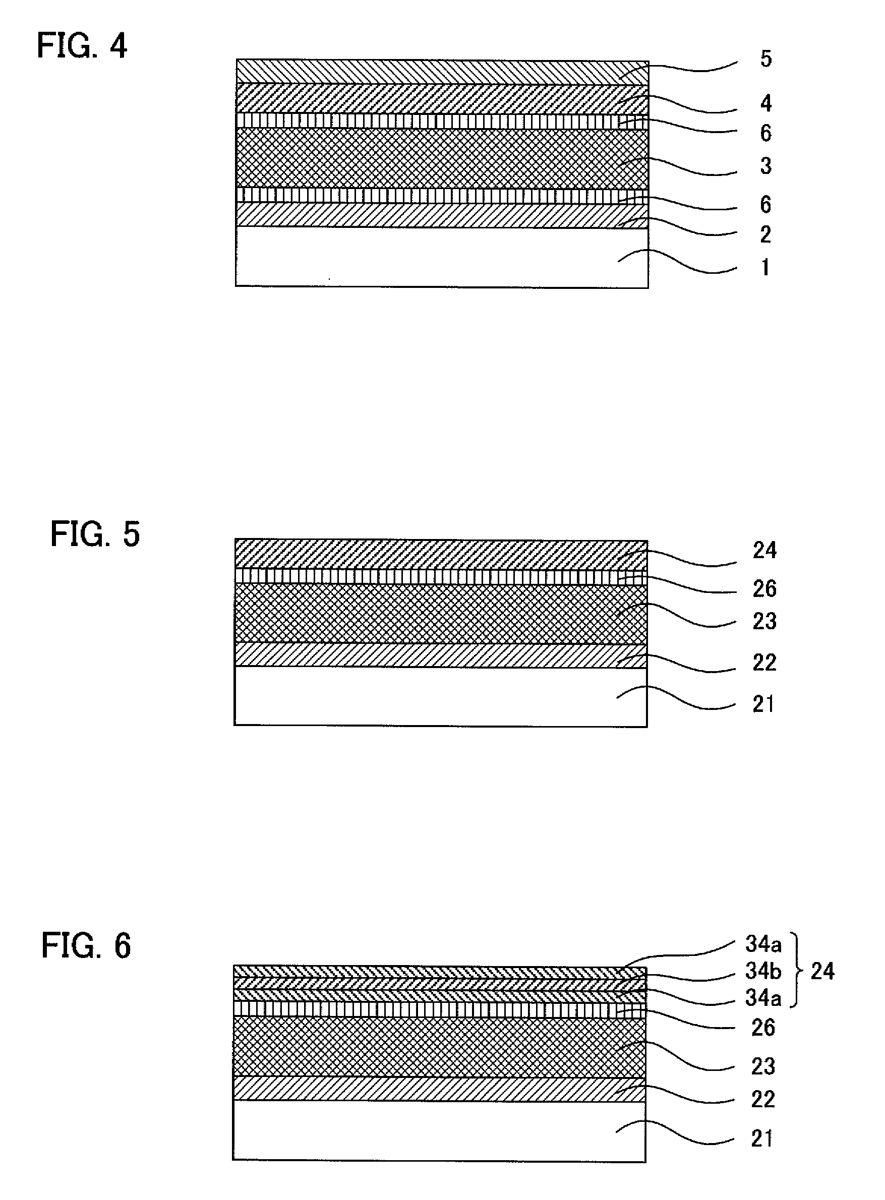
[0158]Next, the second embodiment of the organic EL element of the present invention will be explained. The second embodiment of the organic EL element of the present invention is characterized in comprising: a substrate; an electrode layer formed on the substrate; an organic electroluminescent layer which is formed on the electrode layer and has at least a light emitting layer; and a semiconductor electrode layer which is formed on the organic electroluminescent layer and contains an organic compound having a band gap of 2.0 eV or more and a metal.

[0159]The organic EL element of the present embodiment will be explained by referring to the drawings. FIG. 5 is a schematic cross-sectional view showing one example of the organic EL element of the present embodiment. In FIG. 5, an organic EL element comprises: a substrate 21; an electrode layer 22 formed on the substrate 21; an organic EL layer 23 which is formed on the electrode layer 22 and has at least a light emi...

example 1

Formation of First Electrode Layer

[0198]As a substrate, a transparent glass substrate having a size of 40 mm×40 mm and a thickness of 0.7 mm (alkaliless glass NA35 manufactured by NH Technoglass) was prepared, this transparent glass substrate was cleaned according to a conventional method, and a thin film of an indium zinc oxide compound (IZO) (thickness 130 nm) was formed as an anode on the transparent glass substrate by a sputtering method. Upon formation of the IZO thin film, a mixed gas of Ar and O2 (volume ratio Ar:O2=100:1) was used as a sputtering gas, and a pressure of 0.1 Pa and a DC output of 150 W were used. Further, a photosensitive resist (OFPR-800 manufactured by Tokyo Ohka Kogyo Co., Ltd.) was coated on the IZO thin film (anode), and mask exposure, development (using NMD3 manufactured by Tokyo Ohka Kogyo Co., Ltd.) and etching were performed to pattern an IZO thin film (anode).

(Formation of Hole Injecting / Transporting Layer)

[0199]The aforementioned transparent glass s...


PUM


Abstract

A main object of the present invention is to provide an organic EL element which can ease damages of an organic EL layer upon formation of an electrode layer, and enables display of a high quality image. The present invention attains the above object by providing an organic electroluminescent element comprising: a substrate; a first electrode layer formed on the substrate; an organic electroluminescent layer which is formed on the first electrode layer, and has at least a light emitting layer; a semiconductor buffer layer which is formed on the organic electroluminescent layer, and contains an inorganic compound having a band gap of 2.0 eV or more and a metal; and a second electrode layer formed on the semiconductor buffer layer.

Description

BACKGROUND OF THE INVENTION[0001]1. Field of the Invention[0002]The present invention relates to an organic electroluminescent (herein after, may be abbreviated as organic EL) element.[0003]2. Description of the Related Art[0004]The organic EL element has an advantage that visibility is high due to self light emission, impact resistance is excellent, different from a liquid crystal display, due to a wholly solid display, a response rate is rapid, scarcely influenced by a temperature change, and a visual angle is large. Utility as a light emitting element in an image displaying apparatus attracts attention.[0005]The organic EL element has a fundamental construction of a laminated structure of anode / light emitting layer / cathode, and a construction in which an anode as a transparent electrode is formed on a substrate such as a glass substrate is usually adopted. In this case, emitted light is taken out from the substrate side (anode side).[0006]On the other hand, in recent years, an at...

Claims


Application Information

Patent Timeline
Patent Type & Authority Applications(United States)
IPC IPC(8): H01J1/62H01L51/50H01L51/52H05B33/26H05B33/12H05B33/14
CPCH01L51/5092Y10S428/917H01L51/5221H01L51/5206H10K50/17H10K50/171H10K50/81H10K50/816H10K50/82
Inventor MORI, TOSHITAKAOHYAGI, YASUYUKIKIDO, JUNJI
Owner DAI NIPPON PRINTING CO LTD
Why Eureka
Try Eureka