

Light emitting element and a manufacturing method thereof
a technology of light emitting elements and manufacturing methods, which is applied in the direction of excavations, foundation engineering, roads, etc., can solve the problems of reducing the light output of the led, limiting the scattering of light, and limiting the light generation of the led, so as to improve the light extraction efficiency of the led, improve the scattering effect, and improve the quality
- Summary
- Abstract
- Description
- Claims
- Application Information
AI Technical Summary
Benefits of technology
Problems solved by technology
Method used
Image

Examples
first embodiment
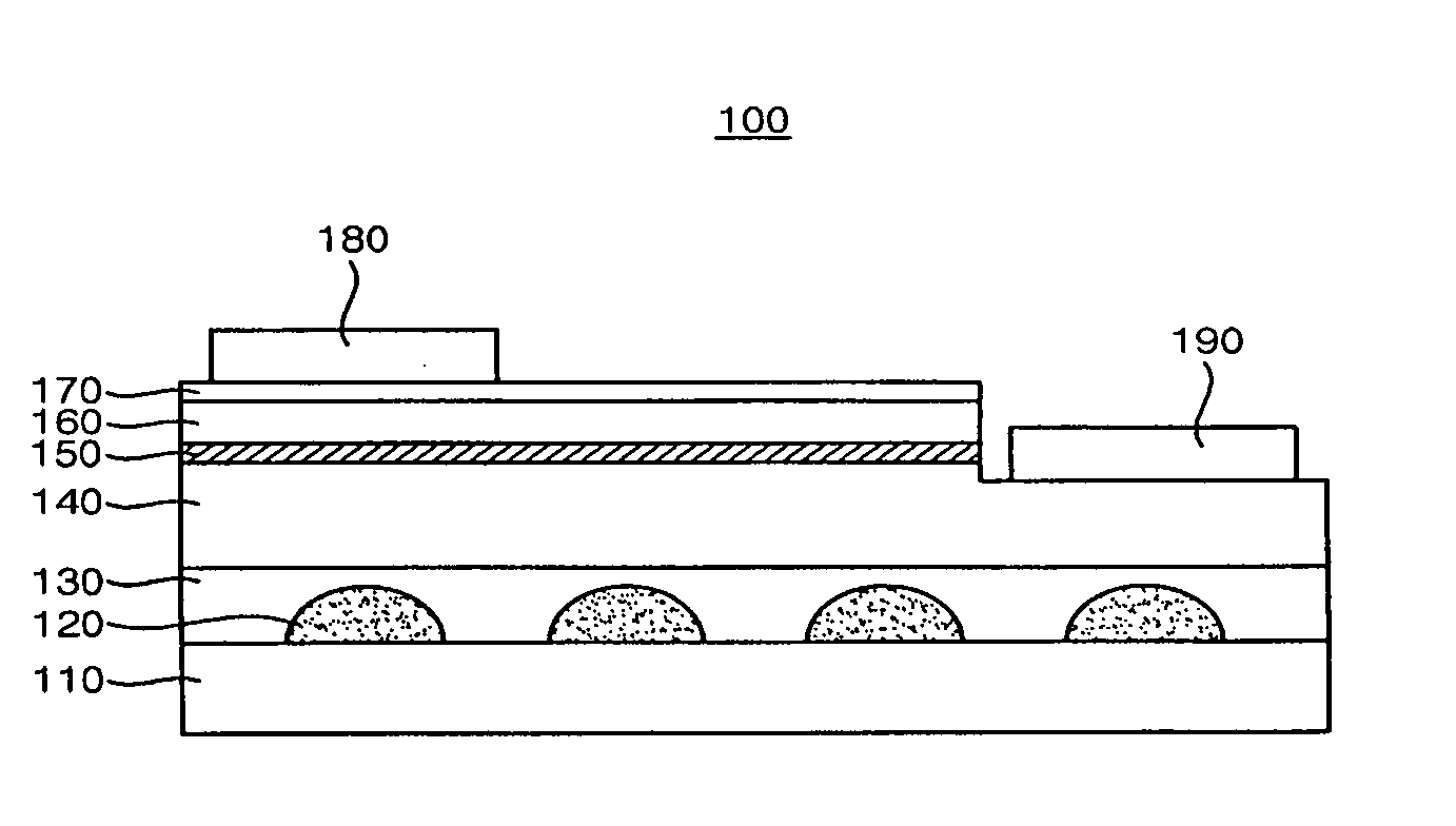
[0063]FIG. 4 is a cross sectional view schematically illustrating a GaN-based LED in accordance with the present invention.
[0064]As shown in FIG. 4, a GaN-based LED 100 in accordance with the first embodiment of the present invention comprises a substrate 110, a dielectric thin film 120, a buffer layer 130, an n-type GaN layer 140, an active layer 150, a p-type GaN layer 160, a current spreading layer 170, a p-electrode 180, and an n-electrode 190. During an operation, an electron-hole recombination occurs in the active layer 150, to generate a light when a current flows through the p-electrode 180 and the n-electrode 190
[0065]Generally, a MOCVD (Metal Organic Chemical Vapor Deposition) apparatus is used to grow the GaN layer on the substrate 110. The substrate 110 comprises, but not limited to a sapphire substrate or a silicon carbide substrate. The substrate 110 may comprises one of a quartz, an AlGaInN, an AlGaN, an InGaN, an AlN, a BN, a CrN, a TiN, and a GaAs.
[0066]The dielectr...
second embodiment
[0085]FIGS. 8 and 9 are a plane view and a cross-sectional view respectively, showing a structure of a GaN-based LED in accordance with the present invention wherein a dielectric thin film includes a pentagonal embossed pattern comprising a SiON in particular. For convenience of description, only the dielectric thin film disposed on the substrate is shown.
[0086]As shown in FIGS. 8 and 9, an LED 300 in accordance with the second embodiment of the present invention comprises a substrate 310 and a dielectric thin film 320 having a pentagonal embossed pattern disposed on the substrate 310. A thickness of the pentagonal embossed pattern of the dielectric thin film 320 ranges from 1 to 5 μm, an average diagonal distance thereof ranges from 1 to 10 μm, and a distance therebetween ranges from 1 to 10 μm. The term “average diagonal distance” refers to a distance between a vertex and an opposing side. The dielectric thin film comprises a SiOxNy having a refractive index of approximately 1.78....
third embodiment
[0089]FIGS. 10 and 11 are a plane view and a cross-sectional view respectively, showing a structure of a GaN-based LED in accordance with the present invention wherein a dielectric thin film includes a hexagonal embossed pattern comprising a SiON in particular. For convenience of description, only the dielectric thin film disposed on the substrate is shown.
[0090]As shown in FIGS. 10 and 11, an LED 400 in accordance with the third embodiment of the present invention comprises a substrate 410 and a dielectric thin film 420 having a hexagonal embossed pattern disposed on the substrate 410. A thickness of the hexagonal embossed pattern of the dielectric thin film 420 ranges from 1 to 5 μm, an average diagonal distance thereof ranges from 1 to 10 μm, and a distance therebetween ranges from 1 to 10 μm. The term “average diagonal distance” refers to a distance between a vertex and an opposing vertex. The dielectric thin film comprises a SiOxNy having a refractive index of approximately 1.7...
PUM
 Abstract
Description
Claims
Application Information