Bolometer
- Summary
- Abstract
- Description
- Claims
- Application Information
AI Technical Summary
Benefits of technology
Problems solved by technology
Method used
Image

Examples
Embodiment Construction
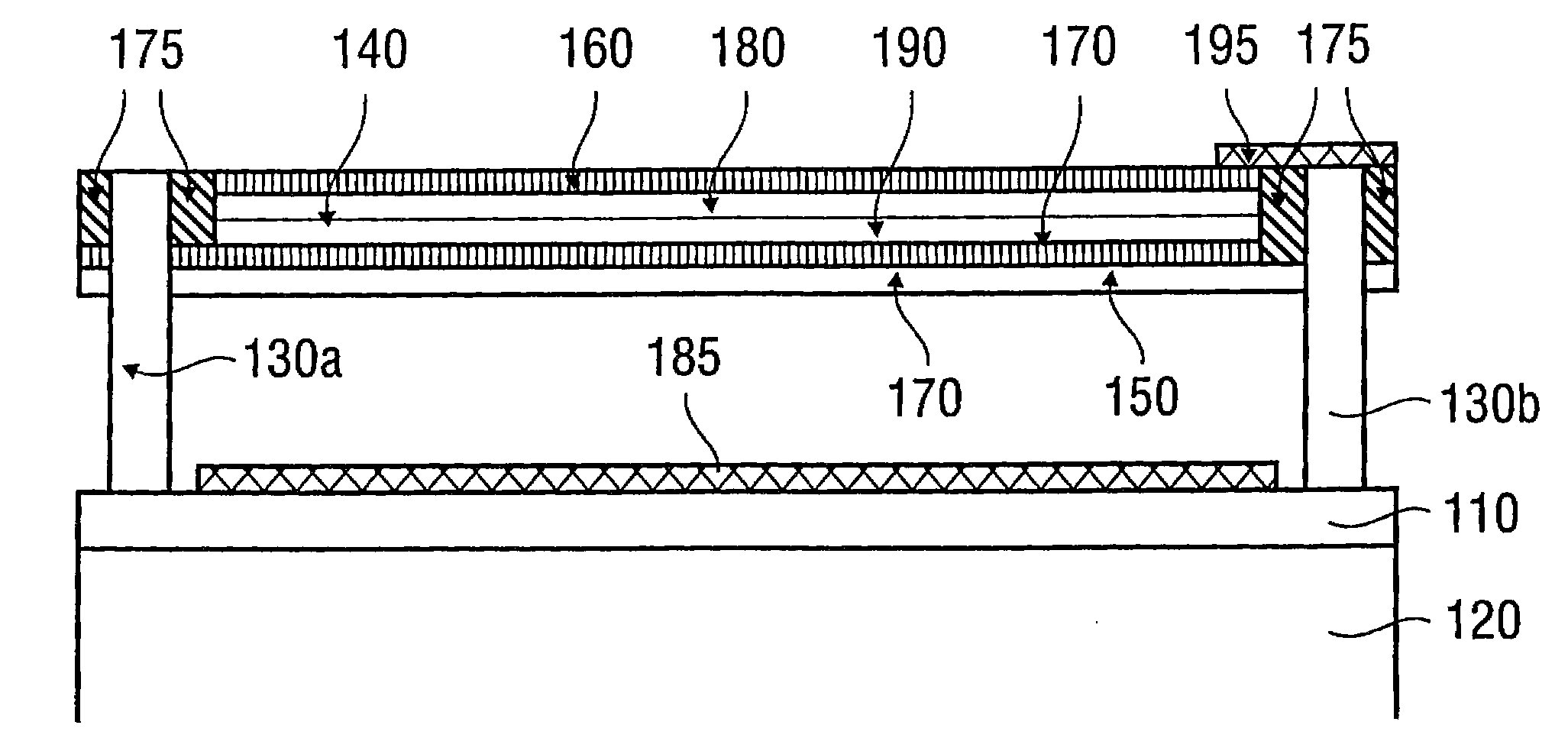
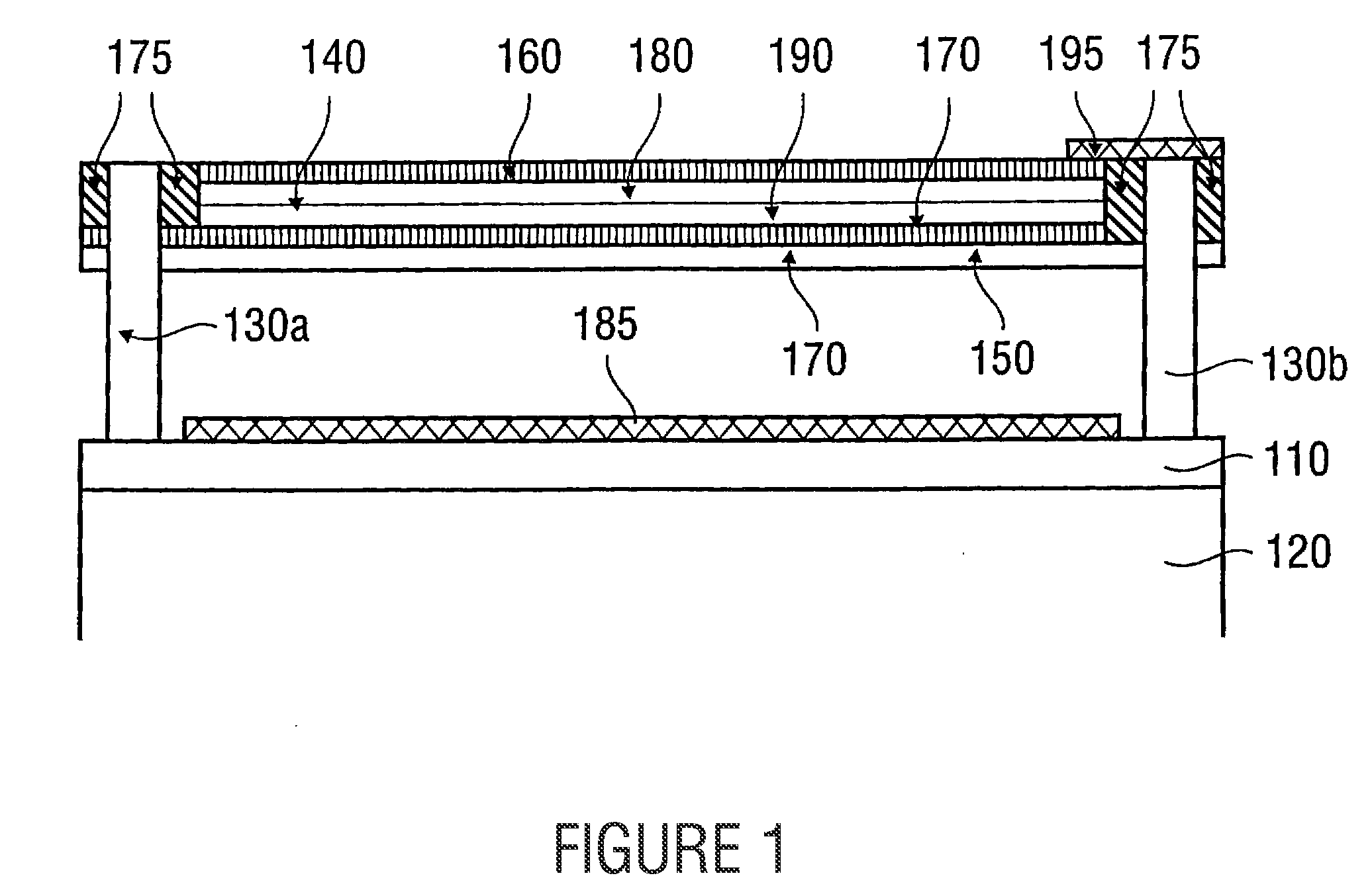
[0028]In the embodiment of FIG. 1 described in the following, as opposed to the structure of FIG. 3, the membrane is replaced by a layer arrangement of silicon nitride and / or silicon oxide as a non-conducting support, on which a p-n or p-i-n diode is disposed as a multilayer system of organic semiconductor layers.
[0029]In the bolometer of FIG. 1, a planar non-conducting background 110, e.g. a layer of silicon oxide, is provided on a substrate such as a silicon wafer 120, for example. The layer 110 may be the polished top oxide layer on a CMOS wafer, for example, which contains all layers and structures needed for a CMOS circuit underneath the surface, wherein the CMOS circuit forms evaluation electronics of the bolometer, for example.
[0030]Two spacers 130 project from the non-conducting background 110 and support a membrane 140 at their ends facing away from the substrate 120. By being suspended between the two spacers 130, the membrane 140 is therefore located above the background ...
PUM
 Abstract
Description
Claims
Application Information
 - Generate Ideas
- Intellectual Property
- Life Sciences
- Materials
- Tech Scout
- Unparalleled Data Quality
- Higher Quality Content
- 60% Fewer Hallucinations
Browse by: Latest US Patents, China's latest patents, Technical Efficacy Thesaurus, Application Domain, Technology Topic, Popular Technical Reports.
© 2025 PatSnap. All rights reserved.Legal|Privacy policy|Modern Slavery Act Transparency Statement|Sitemap|About US| Contact US: help@patsnap.com