On Chip Antenna And Method Of Manufacturing The Same

Inactive Publication Date: 2009-04-02
DOAN MY THE
View PDF1 Cites 42 Cited by
  • Summary
  • Abstract
  • Description
  • Claims
  • Application Information

AI Technical Summary

Benefits of technology

[0014]It is therefore an object of the present invention to

Problems solved by technology

Any antennas fabricated on silicon substrate would have substrate effects in the millimeter wave range that would reduce the antenna efficiency.
The doped silicon substrate that often found in standard CMOS and Bipolar integrated circuits is considered as lossy, due to its resistive conductivity.
With a resistive conductive substrate, this leakage substrate current would result in a resistive power loss.
So again a percentage of the signal would be loss.
In addition to giving rise to power loss, according to Lenz's law, eddy currents create their own magnetic fields that is in the opposite direction of those of the signal line.
However, each one of these methods does have its drawbacks.
1961-1968, 1997, is expensive, has much higher crystal defects, and increases latch up.
However, with high resistivity silicon in the “handle” substrate (below the buried oxide) in a silicon-on-insulator, SOI, wafer, the crystal defects and latch up

Method used


Image

  • On Chip Antenna And Method Of Manufacturing The Same
  • On Chip Antenna And Method Of Manufacturing The Same
  • On Chip Antenna And Method Of Manufacturing The Same

Examples


Embodiment Construction

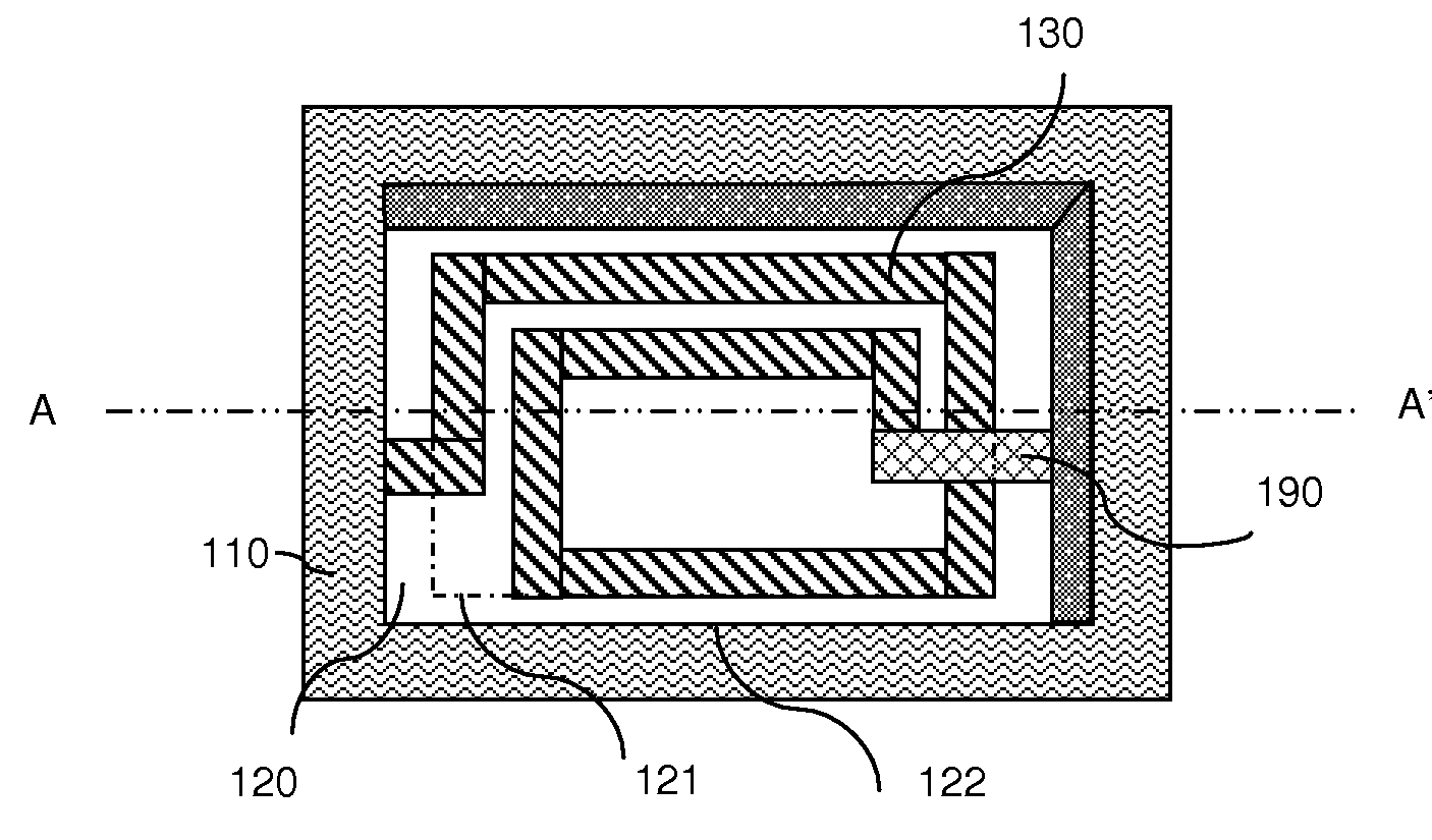
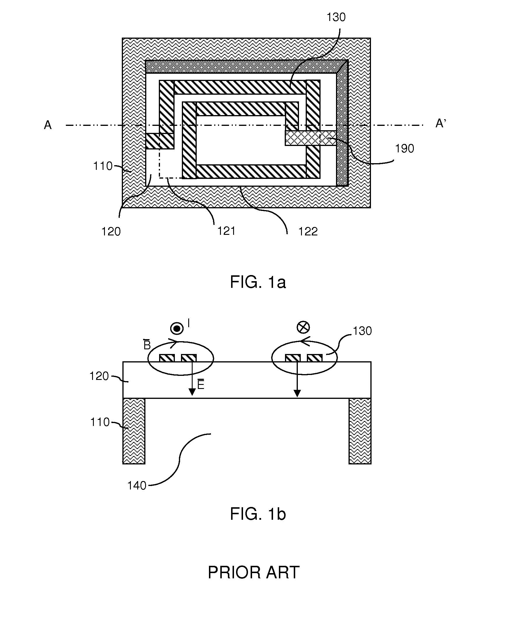
[0031]Referred now to FIGS. 1a and b, a prior art that used back side micro-machining to remove the silicon substrate, 110, under an inductor. The prior art belongs to Ozgur et al as mentioned in the background section. FIG. 1a is a bottom view of the inductor. FIG. 1b is a side view of the cross-sectional cut at A-A′ in FIG. 1a. An air-filled trench, 140, is formed under the inductor after the silicon is removed. It is important to point out that the area of the trench as defined by the boundary, 122, is larger than that of the inductor. The area of the inductor, 121, is defined by the boundary of outer edge of the outermost line of the inductor, 130. In another word, all the silicon inside the boundary 122 is removed. As the authors pointed out, for large inductor they encounter stress problem. To resolve this issue, the authors deposit a stress compensation layer on top of the inductor before doing the back side micromachining. They were able to build a 2 mm×3 mm suspended induct...


PUM


Abstract

An antenna with air-filled trench is integrated with a radio frequency (RF) circuit. The trench locates directly under the metal lines that made up the antenna and is formed by etching from the back side of the semiconductor substrate until all the substrate material in the trench is removed. The air-filled trench greatly reduces the losses due to the semiconductor substrate; therefore the performance of the antenna improves greatly. When the antenna is a large planar spiral inductor, the air-filled trench means the semiconductor substrate inside the spiral inductor is untouched; hence integrated circuit can be built inside the antenna and on that substrate. Therefore the RF integrated circuit has a smaller size. Air-filled trench can also be used to reduce the semiconductor substrate noise coupling between digital circuit block and analog/RF circuit block. This air-filled trench and the air-filled trench under the antenna are formed at the same time.

Description

CROSS REFERENCE TO RELATED APPLICATIONS[0001]This application claims the benefit of U.S. provisional Patent Application No. 60 / 976,412, filed Sep. 29, 2007, the contents of which are hereby incorporated by reference as if stated herein.BACKGROUND OF THE INVENTION[0002](1) Field of the Invention[0003]The present invention generally relates to a wireless integrated circuit having an embedded antenna on chip. More particularly, this invention relates to the design and manufacturing of the embedded antenna with air-filled trench that would improve the performance of the wireless integrated circuit while reducing cost.[0004](2) Description of the Prior Art[0005]For short range, and low power transceivers, on chip antennas are preferred as they generally offer lower cost and higher reliability when compare to off chip antennas. Typically, there are two methods of transmitting electromagnetic waves (or signals) between the transmitter and the receiver: backscattering and inductive coupling...

Claims


Application Information

Patent Timeline
IPC IPC(8): H01L31/00H01L21/02
CPCG06K19/07749G06K19/07775G06K19/07779H01L23/5227H01L28/10H01L2924/3011H01Q1/2225H01L2924/0002H01Q1/2283H01Q7/00H01Q23/00H01L2924/00
Inventor DOAN, MY THE
Owner DOAN MY THE
Why Eureka
Try Eureka