Wiring board

Active Publication Date: 2009-04-02
SHINKO ELECTRIC IND CO LTD
View PDF5 Cites 17 Cited by
  • Summary
  • Abstract
  • Description
  • Claims
  • Application Information

AI Technical Summary

Benefits of technology

[0020]According to the present invention, when the impurity concentration of the semiconductor substrate is low to such an extent that an inversion layer is generated within the semiconductor substrate 17 by a potential difference between the through electrodes and the semiconductor substrate upon applying power, the first guard ring is formed so as to have the same conductivity type as that of the semiconductor substrate. In this case, generation of the inversion layer is prevented by the first guard ring formed to surround side surfaces of the through electrode. Further, it can be prevented that the inversion layer generated around the through electrode is electrically connected to the first conductivity-type impurity diffusion layer. Thus, an increase in leakage current is suppressed, and hence characteristic deterioration of a semiconductor element formed in the semiconductor substrate can be prevented.
[0021]When the impurity concentration of the semiconductor substrate is high to such an extent that an inversion layer is not generated within the semiconductor substrate 17 by a potential difference between the through el

Problems solved by technology

This leads to an increase in a leakage current of the element.
T

Method used


Image

  • Wiring board
  • Wiring board
  • Wiring board

Examples


first embodiment

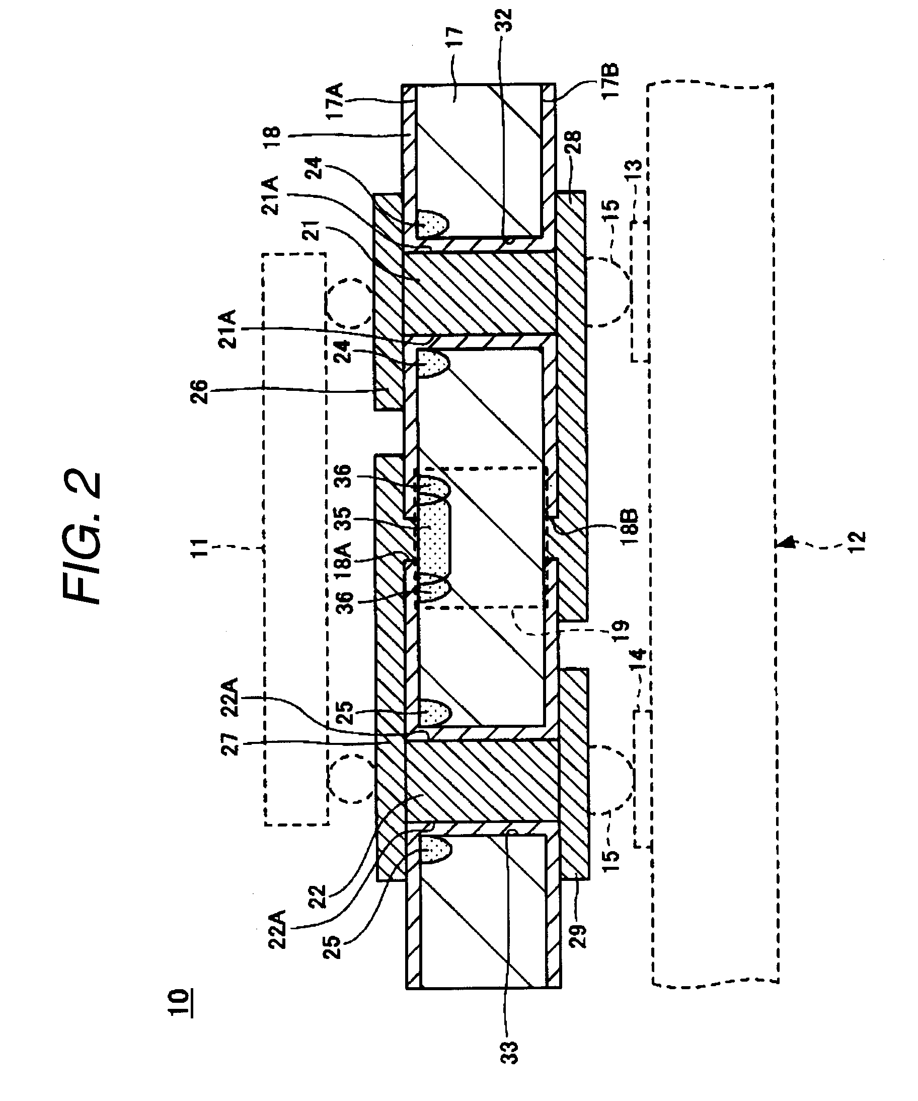
[0042]FIG. 2 is a cross-sectional view of a wiring board according to a first embodiment of the present invention.

[0043]By reference to FIG. 2, a wiring board 10 of a first embodiment includes: a semiconductor substrate 17; an insulating film 18; a Zener diode 19 serving as a semiconductor element; through electrodes 21 and 22; first guard rings 24 and 25; wirings 26 and 27 serving as first wirings; and wirings 28 and 29 serving as second wirings.

[0044]The semiconductor substrate 17 is almost shaped like a rectangular thin board, and made of a semiconductor material such as silicon. The semiconductor substrate 17 has through holes 32 and 33 formed at predetermined locations thereon. Conditions for forming the semiconductor substrate 17, an impurity diffusion layer formed in the semiconductor substrate 17, guard rings, and the like, will be described later.

[0045]The insulating film 18 has an opening 18A through which an upper surface of a first conductivity type impurity diffusion la...

second embodiment

[0100]FIG. 14 is a cross-sectional view of a wiring board according to a second embodiment of the present invention. In FIG. 14, constituent elements identical with those of the structure shown in FIG. 2 are assigned the same reference numerals.

[0101]By reference to FIG. 14, a wiring board 50 of the second embodiment is configured almost in the same manner as the wiring board 10 of the first embodiment (see FIG. 2) except that a second guard ring 51 is provided.

[0102]The second guard ring 51 is formed in frame shape on the upper surface 17A of the semiconductor substrate 17 to surround the first conductivity type impurity diffusion layer 35, the impurity diffusion layer 36, the through electrodes 21 and 22, and the first guard rings 24 and 25. Specifically, the second guard ring 51 is formed along the side surface 17C of the semiconductor substrate 17 and hereby positioned so as to surround the first conductivity type impurity diffusion layer 35, the impurity diffusion layer 36, the...


PUM


Abstract

There is provided a wiring board. The wiring board includes: a semiconductor substrate having a through hole and covered with an insulating film; a through electrode formed in the through hole; a first wiring connected to one end of the through electrode; and a second wiring connected to the other end of the through electrode. The semiconductor substrate includes: a semiconductor element and a first guard ring formed to surround the through hole. The semiconductor element includes a first conductivity-type impurity diffusion layer having a different conductivity-type from that of the semiconductor substrate and is electrically connected to the first wiring and the second wiring.

Description

[0001]This application is based on and claims priority from Japanese Patent Application No. 2007-257504, filed on Oct. 1, 2007, the entire contents of which are hereby incorporated by reference.BACKGROUND OF THE INVENTION[0002]1. Technical Field[0003]The present disclosure relates to a wiring board including a through electrode passing through a semiconductor substrate and being insulated from the semiconductor substrate and a wiring connected to one end of the through electrode and being electrically connected to an electronic component.[0004]2. Related Art[0005]A wiring board 200 shown in FIG. 1 has hitherto been used as a re-wiring board (an interposer) for electrically connecting a semiconductor chip to a mounting board such as a mother board.[0006]FIG. 1 is a cross-sectional view of a wiring board in the related-art.[0007]By reference to FIG. 1, the related-art wiring board 200 includes a semiconductor substrate 206 corresponding to a base-body, an insulating film 207, through ...

Claims


Application Information

Patent Timeline
IPC IPC(8): H01L21/768H01L29/866H01L23/538
CPCH01L23/481H01L23/585H01L23/60H01L2224/16225H01L25/16H01L2225/06527H01L23/62
Inventor MURAYAMA, KEINAKAJIMA, SHINJI
Owner SHINKO ELECTRIC IND CO LTD
Why Eureka
Try Eureka